
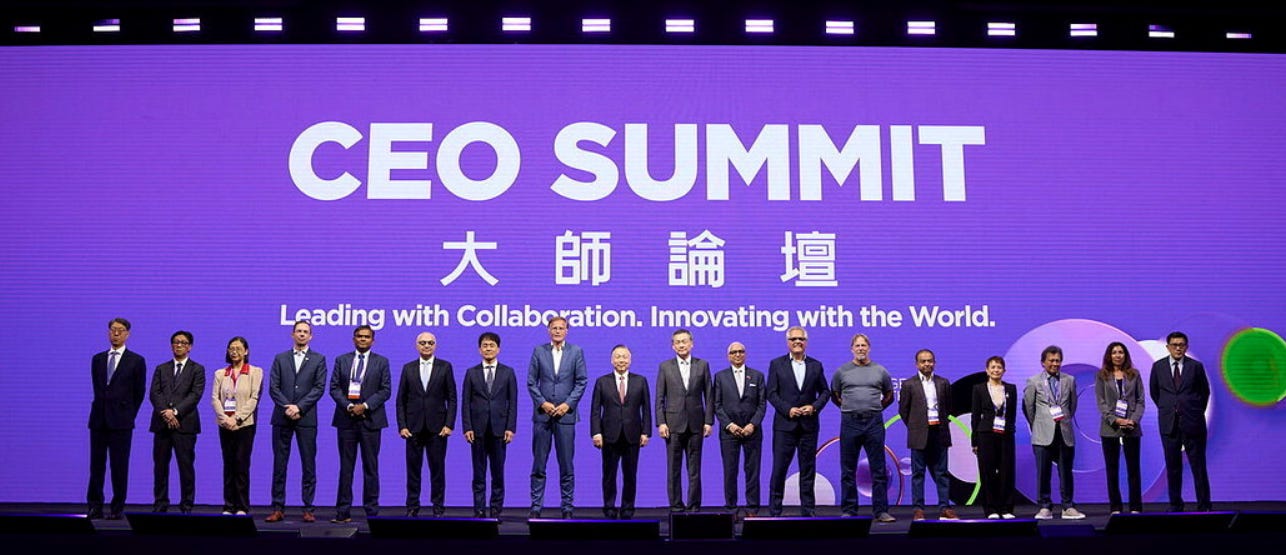
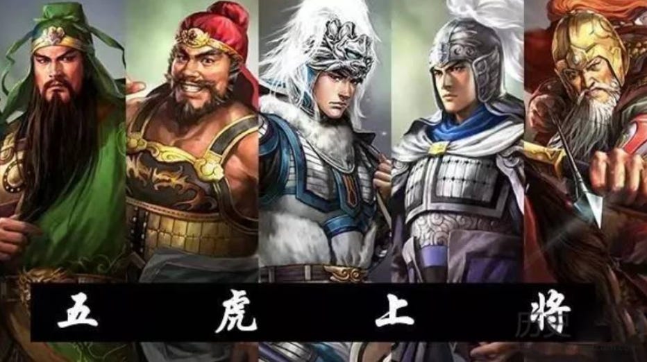
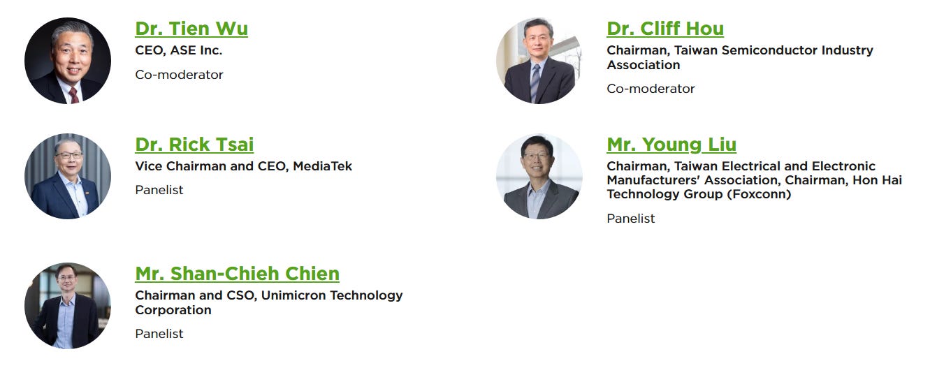
SEMICON Taiwan 2026 will feature an unusual lineup: TSMC, ASE, MediaTek, Unimicron, and Hon Hai/Foxconn appearing together in the same discussion. Taiwanese media has labeled them the semiconductor industry’s “Five Tigers.” The term is not an official industry classification, but the analogy is useful. In Chinese history and popular culture, the “Five Tiger Generals” referred to five leading commanders who fought on different fronts but collectively formed the military core of the same camp. Taiwan’s five companies play a similar role in AI infrastructure: they are not direct competitors, but each controls a different and increasingly critical layer of the hardware stack.
MediaTek represents AI ASIC design, TSMC advanced logic manufacturing, ASE advanced packaging and test, Unimicron high-end ABF substrates and PCBs, while Foxconn sits at the system level, integrating processors, networking, power, cooling, and mechanical infrastructure into deployable AI servers and racks. Viewed together, the five companies provide a useful framework for understanding why Taiwan’s position in AI is much broader than wafer fabrication alone.
That distinction matters because the AI infrastructure race is no longer simply about who can secure the most GPUs. The bottlenecks are migrating across the stack, from HBM and advanced packaging to substrates, optical connectivity, power delivery, liquid cooling, rack integration, and eventually the construction of entire data centers. The competitive unit is gradually moving from the chip to the package, from the package to the rack, and from the rack to the AI factory. That is the backdrop against which these “Five Tigers” should be analyzed.
MediaTek is still primarily associated with smartphone SoCs, but that description is becoming increasingly incomplete. The more strategically important part of the company’s roadmap is its expansion into AI data-center ASICs, where hyperscalers are looking for alternatives to a purely merchant-GPU architecture. These customers are not necessarily trying to replace NVIDIA across every workload. Instead, they are developing custom silicon for workloads where they can improve cost, power efficiency, memory architecture, networking, or software control relative to a general-purpose accelerator.
This creates a very different opportunity from the traditional mobile semiconductor market. Building a competitive AI ASIC requires much more than RTL design. It requires access to leading-edge process technology, advanced SerDes, HBM integration, chiplets, advanced packaging, and increasingly close coordination with system-level power and networking architectures. MediaTek has accumulated many of these capabilities through years of designing complex mobile and connectivity SoCs, making its move into data-center silicon more credible than it might initially appear.
The key question for investors is not whether custom ASICs will replace GPUs. NVIDIA’s ecosystem remains extraordinarily difficult to displace because its advantage extends well beyond silicon into CUDA, networking, rack-scale architecture, and software. The more relevant question is how much incremental AI compute will migrate toward custom accelerators developed by Google, Amazon, Meta, Microsoft, and other hyperscalers. Even if GPUs remain dominant, a relatively modest shift in incremental workloads toward custom silicon could create a very large addressable market for MediaTek and Taiwan’s broader ASIC ecosystem.
This is why MediaTek deserves more attention at SEMICON Taiwan. The company is increasingly moving from a mobile-chip narrative toward an infrastructure-silicon narrative. If this transition succeeds, it could become one of the more important structural changes in Taiwan’s semiconductor landscape over the next several years.
TSMC’s importance to AI is obvious, but the nature of that importance is changing. The conventional description of TSMC as a semiconductor foundry is becoming too narrow because modern AI accelerators depend not only on leading-edge transistors, but also on HBM integration, silicon interposers, redistribution layers, advanced bonding, chiplets, and increasingly complex packaging architectures.
The result is that the manufacturing problem is expanding from wafer fabrication into system integration. CoWoS is the most visible example. During the early phase of the generative-AI boom, GPU availability was often described as the central constraint. That quickly shifted to HBM, then to CoWoS, and now the bottleneck is becoming more distributed across interposers, substrates, thermal design, test capacity, optical connectivity, and package yield.
This changes what TSMC is effectively selling. A next-generation AI accelerator is less like a conventional monolithic semiconductor and more like a miniature computing system assembled within a package. As compute dies, I/O dies, HBM stacks, interposers, and eventually optical engines are integrated more tightly, advanced packaging becomes part of processor architecture rather than a downstream manufacturing step.
For that reason, the most important question at SEMICON Taiwan is no longer simply how much additional CoWoS capacity TSMC plans to add. The more fundamental issue is how large and complex an AI package can become before existing manufacturing architectures encounter physical or economic limits. The answer will determine demand for new bonding tools, inspection systems, substrate materials, thermal interfaces, panel-level packaging, and potentially optical I/O. In other words, TSMC’s evolution is increasingly pushing the industry toward what can be described as system foundry economics.
AI has also changed the strategic position of OSAT companies. Historically, much of the semiconductor industry’s value creation was perceived to sit toward the front end: design the chip, fabricate the wafer, and then send it downstream for packaging and testing. That hierarchy is becoming less accurate because packaging is now one of the primary determinants of how much compute, memory, and I/O can be integrated into a usable AI system.
This makes advanced packaging part of processor architecture. ASE’s VIPack platform, for example, spans advanced redistribution, fan-out, 2.5D and 3D integration, and heterogeneous chiplet architectures. The strategic value of these technologies increases as AI packages grow larger and more complex, because package size directly affects yield, warpage, thermal behavior, routing density, and assembly economics.
Panel-level packaging is particularly interesting in this context. Wafer-level processes work extremely well when package dimensions remain relatively small, but AI accelerators are moving in the opposite direction. More compute dies, more HBM stacks, more I/O, and larger interposers all increase the pressure to process larger rectangular areas more efficiently. At some point, the economics of fabricating very large packages on circular wafers becomes increasingly uncomfortable, which is one reason panel-level approaches continue to attract attention.
For ASE, the strategic question is therefore not simply how much advanced packaging TSMC may outsource. The more important issue is whether ASE can develop architectures and manufacturing platforms that are complementary to, rather than merely downstream from, TSMC’s packaging roadmap. If that happens, the role of OSAT could move from manufacturing support back into the critical path of AI system development.
ABF substrates are easy to underestimate because they appear passive compared with GPUs, HBM, or advanced packaging. In reality, larger AI accelerators are turning the substrate into an increasingly difficult engineering problem. As more compute dies and HBM stacks are integrated into a single package, the substrate must support higher routing density, more I/O, greater layer counts, tighter line-and-space requirements, and increasingly severe mechanical and thermal stresses.
Package growth is especially important. Larger substrates make warpage harder to control, while higher-speed electrical interfaces tighten signal-integrity requirements. At the same time, more layers, more vias, and larger panel areas reduce manufacturing margin for error. These effects compound one another, meaning that the substrate can become a limiting factor even when silicon and HBM are available.
This is why the most useful question for Unimicron is not simply whether ABF pricing will rise. The more important issue is how large next-generation AI substrates need to become and what material systems can support that scaling. Once package dimensions move higher, the implications extend well beyond substrate makers themselves. Demand shifts upstream into low-loss glass cloth, ABF films, copper foil, specialty resin systems, drilling and laser equipment, plating, inspection, and potentially glass-core substrates.
The substrate should therefore be viewed as part of the same scaling problem as advanced packaging. Both are responding to the fact that AI processors are becoming physically larger, electrically denser, and mechanically more difficult to manufacture. If the next generation of accelerator packages pushes substrate dimensions substantially higher, this area could become one of the most important bottlenecks in the supply chain.
The first four Tigers can produce world-class semiconductor components, but none of them alone creates usable AI infrastructure. Someone still has to integrate GPUs, CPUs, switches, power systems, cooling hardware, cables, NICs, trays, racks, and management systems into a platform that can operate reliably inside a data center. This is where Foxconn becomes strategically important.
The company is increasingly difficult to describe as simply an electronics manufacturing services provider. AI servers are changing the nature of the product being manufactured. The unit of deployment is moving away from an individual server toward the rack, while the rack itself is becoming a tightly integrated computing system involving power distribution, liquid cooling, high-speed networking, mechanical design, and increasingly complex system validation.
This is particularly important as NVIDIA moves from standalone GPU platforms toward rack-scale architectures. Blackwell accelerated this transition, and Rubin is likely to push it further. The challenge for ODMs is no longer simply to assemble a motherboard inside a chassis; it is to coordinate a complete system in which power, thermals, networking, and compute architecture all constrain one another.
The strategic question is therefore whether companies such as Foxconn remain primarily manufacturing partners or evolve into infrastructure integrators capable of delivering increasingly complete AI factories. If customers begin procuring not only servers or racks but megawatt-scale computing blocks, the value captured by system integrators could rise materially. In that scenario, Foxconn’s role would move further upstream in system design and further downstream into data-center deployment at the same time.
The most interesting part of SEMICON Taiwan this year may not be any single new piece of equipment. The more important signals are likely to come from how different parts of the AI supply chain are beginning to constrain one another.
The first issue is the speed at which custom ASIC demand is growing. GPUs will remain central to AI infrastructure, but hyperscaler silicon programs are multiplying, and that trend benefits not only design houses such as MediaTek but also foundries, HBM suppliers, substrate vendors, advanced packaging companies, and test-equipment makers. Custom ASIC does not need to displace NVIDIA to become one of the semiconductor industry’s largest growth markets.
The second issue is whether advanced packaging remains the industry’s dominant scaling constraint. The semiconductor industry has responded to slowing monolithic scaling by integrating more compute and memory at the package level, but this does not eliminate bottlenecks; it moves them. HBM, interposers, bonding, substrates, package yield, thermal management, and test capacity are increasingly interconnected. The manufacturing chain is no longer linear, because limitations in one layer can quickly propagate across the entire system.
The third issue is package size. Larger packages offer more routing resources, more memory bandwidth, and more compute integration, but they also worsen warpage, thermal stress, substrate complexity, and yield. This is why technologies such as larger interposers, panel-level packaging, glass substrates, hybrid bonding, and optical I/O deserve attention. Much of the next AI hardware cycle may be determined by how effectively the industry can continue increasing package scale without allowing manufacturing economics to deteriorate too rapidly.
A fourth question is whether the product itself is becoming the rack. The semiconductor industry historically optimized chips, then moved toward optimizing packages, and is now increasingly optimizing entire rack-scale systems. Compute, networking, memory, optics, power, and cooling have to be co-designed, creating opportunities far beyond semiconductor vendors. Power companies, liquid-cooling suppliers, connector makers, cable vendors, rack builders, and system integrators are becoming increasingly strategic participants in the AI infrastructure stack.
The final question, and arguably the most valuable one for investors, is where the next bottleneck will emerge. AI has already created extreme tightness in HBM and CoWoS, and it is putting pressure on high-end PCB materials, advanced substrates, copper foil, glass cloth, power systems, and optical components. The largest opportunities often appear when an item previously treated as a low-value component suddenly becomes capacity-constrained or technologically difficult. SEMICON Taiwan is therefore useful not merely as a showcase of existing winners, but as a place to identify the next part of the system that is becoming physically difficult to build.
The biggest mistake investors can make is to analyze Taiwan’s AI advantage company by company. TSMC is critical, but TSMC alone does not explain Taiwan. Neither do MediaTek, ASE, Unimicron, or Foxconn individually. The deeper advantage is the density of the industrial ecosystem and the speed at which different layers of that ecosystem can interact.
Within a relatively small geographic area, Taiwan contains semiconductor design houses, leading-edge foundries, OSATs, substrate makers, PCB suppliers, ODMs, power-electronics companies, cooling suppliers, connector vendors, test-equipment companies, specialty chemical producers, and precision manufacturing firms. That concentration materially reduces engineering iteration time. When an accelerator requires a larger substrate, substrate vendors can work directly with material suppliers. When warpage becomes a problem, packaging houses, equipment makers, and chemical suppliers can adjust processes in parallel. When rack power rises toward hundreds of kilowatts, server ODMs can redesign with power and cooling companies rather than treating those systems as downstream components.
The advantage is therefore not simply lower manufacturing cost. It is engineering velocity.
This is why the “Five Tigers” framework is useful. MediaTek, TSMC, ASE, Unimicron, and Foxconn are not five versions of the same company. They represent five layers of the same AI infrastructure machine. As AI moves from chip-level competition toward system-level optimization, the value of that coordination increases.
For investors attending SEMICON Taiwan 2026, the objective should therefore not simply be to identify the next fashionable semiconductor technology. The more valuable exercise is to understand where AI systems are becoming physically difficult, expensive, or capacity-constrained to build. Wherever complexity rises fastest, the next bottleneck—and often the next major supply-chain opportunity—is usually not far behind.
Comments
Nothing yet. Say the first thing.
Sign in to join the conversation.