
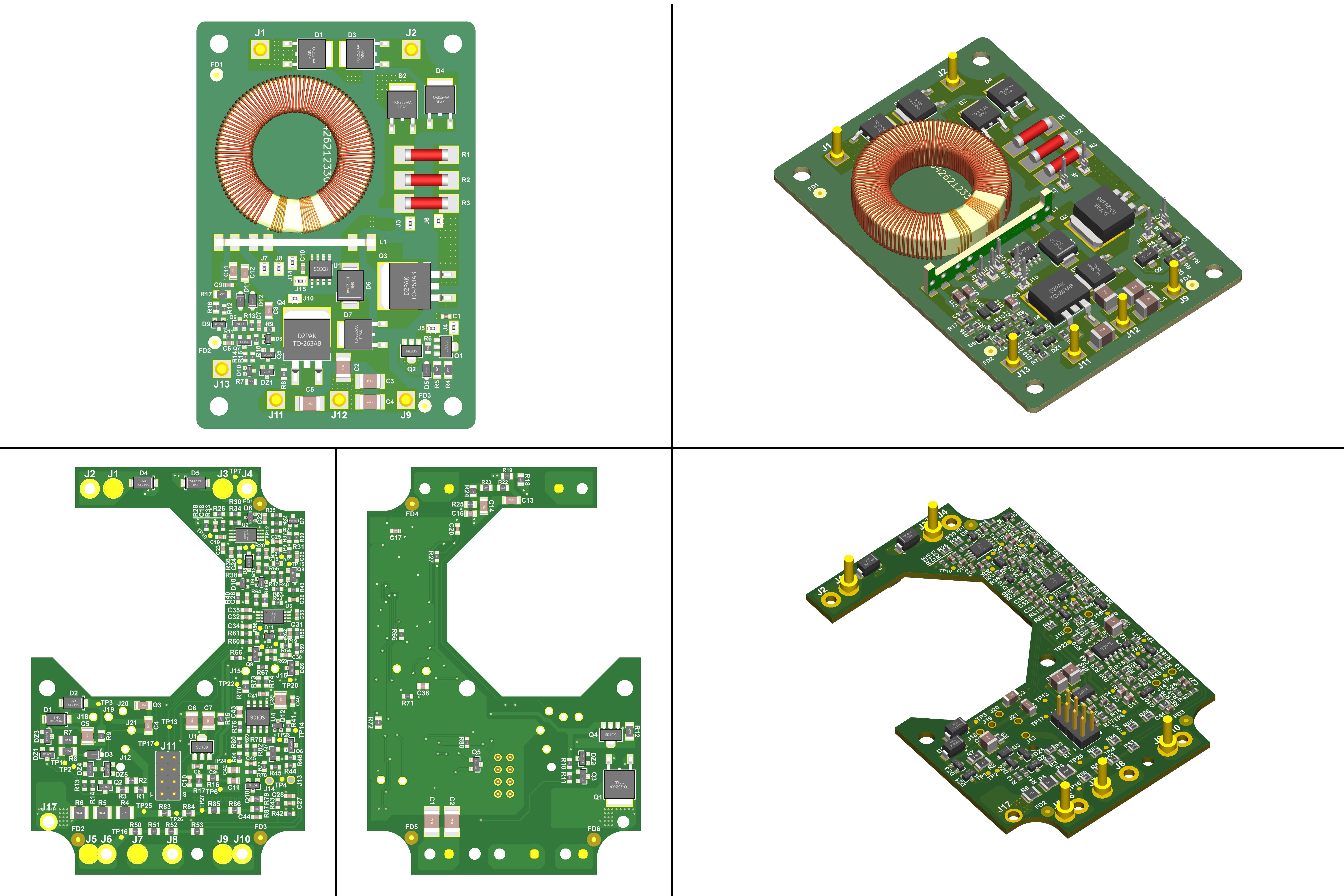
This is a reverse-engineering of the Astec AIT02ZPFC module. The Git repository containing the KiCad project and other resources can be found here.
This article details analyses (read: speculates on) some of the choices that appear to have been made in the design of the PFC module. The first thing you will likely think when looking at the convoluted array of transistor and diode logic circuits contained within this design, is “surely much of this can be greatly simplified with a one-chip solution?”, and you’d be right. The detail to keep in mind however is that sometimes, highly integrated solutions are not always desirable.
It’s clear from the certifications on the cover page of this module’s datasheet, that the primary industry they’re targeting is aerospace and military. In both of these sectors, certification is an expensive ordeal, and if a part goes obsolete and you need to do a complete refactor of the circuit it surrounds, you’re looking down the barrel of another round of very expensive qualification tests. To defend against this, designers will often purposely discretise their circuits which allows them to much more easily substitute simpler building-block parts should they go obsolete. Sure the design will still need to seek minor change approval, but this is far more preferable to requalifying the entire product, as it usually only requires a subset of the tests to be reconducted, often informally. If the part can be sufficiently demonstrated to be a direct drop in (for example, the same basic TL431 shunt regulator, merely from a different manufacturer), the OEM may even be able to push the change through with a change rationale only. All of this helps to keep the production line churning out assemblies with as few hiccups as possible when parts become temporarily or permanently unsourceable.
The other advantage designers get by discretising circuits is an easier process of demonstrating of MTTF/MTBF. Highly integrated solution, while compact, can often be problematic when it comes to obtaining reliability figures from manufacturers. No doubt anyone in this industry will have their ears perk up at the mention of MIL-HDBK-217F. Demonstrating reliability (or at least plausible reliability) is functionally currency in these sectors (whether the figures are hogwash most of the time is a discussion for another time) . So whatever helps pump up those MTTF numbers in the OEM datasheet, is worth doing.
The boost inductor is a custom wound part. It however is not just a plain toroidal core inductor; it has two additional windings. At first I thought they might be using one for sensing/feedback purposes, but what about the other? After mapping out their respective downstream circuits, it became clear these were for auxiliary rails; one for generating a low-voltage supply to the controller board, and the other for driving the N-Channel MOSFET that bypasses the external inrush limiting resistor.
The part number of the core is barely visible through the windings - a Chang Sung CH330060E6.8. The wire gauges for the primary and two secondaries are 24 AWG, 28 AWG, and 30 AWG, respectively. The secondary with 4 turns is 30AWG with thicker insulation for a finished diameter of ~0.4mm. The winding direction/polarity is marked with a dot in the image below.
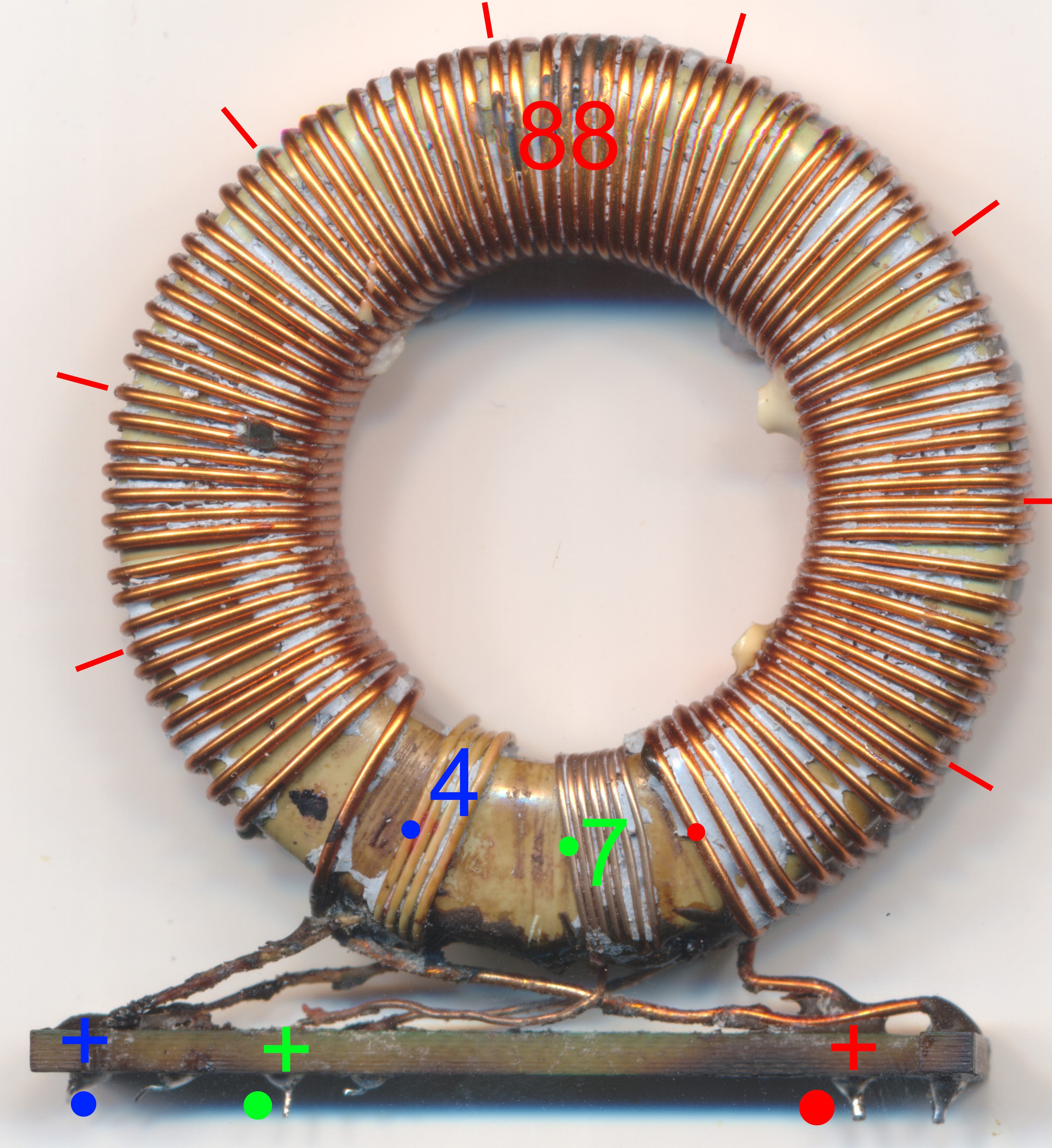
The turns ratios could be easily recovered by simply counting the turns on each winding - 88:7:4. Next I applied a +/-10V, 100kHz (close to the actual boost converter frequency of ~134kHz) sine wave to the primary (88 turns) winding and measured across the two secondary windings. The secondaries were tested both open and terminated with a 1k burden resistor, and output voltages were basically the same. Here is what I got reading off the scope.
VP(88) = 20.2Vpp
VS1(7) = 1.33Vpp
VS2(4) = 750mVpp
Ideal turns ratios are as follows:
VP:VS1 = 88 : 7 = 12.57
VP:VS2 = 88 : 4 = 22
The measured ratios however are:
VP:VS1 = 20.2 : 1.33 = 15.19
VP:VS2 = 20.2 : 0.75 = 26.93
Next I measured the ESR for each winding:
VP(88) = 1.3Ω
VS1(7) = 105mΩ
VS2(4) = 61mΩ
I then tested measured the inductance of each winding under various combinations of shorts/opens on the windings not under test. The table below shows the measured values.
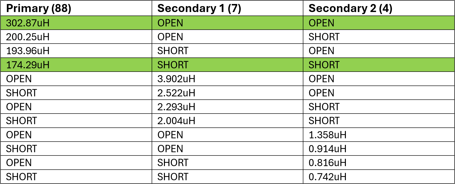
The measurements where all other windings are shorted are the leakage inductances, while measurements with all other windings open are the self/magnetising inductances. For example, the primary winding’s leakage inductance is 174.29uH, while its self/magnetising inductance is 302.87uH.
We can also wire the windings to measure their series-aiding and opposing inductances. Here are those:
LP-S1-AID = 348.19uH
LP-S1-OPP = 266.29uH
LP-S2-AID = 328uH
LP-S2-OPP = 281.75uH
LS1-S2-OPP = 8.112uH
LS1-S2-OPP =2.315uH
These can be used to calculate the coupling factors using the equation below.
\(k_{12} = \dfrac{M_{12}}{\sqrt{L_1L_2}} = \dfrac{L_{12AID} - L_{12OPP}}{4\sqrt{L_1L_2}} \)
Here’s what we get:
kP-S1 = 0.5956
kP-S2 = 0.5701
kS1-S2 = 0.6296
The SPICE directives for simulation are straightforward from here, and follow the basic format:
KPS1 L1P L1S1 0.5956
KPS2 L1P L1S2 0.5701
KS1S2 L1S1 L1S2 0.6296
Where:
L1P = 302.87uH
L1S1 = 3.902uH
L1S2 = 1.358uH
A near-complete LTSPICE schematic of this converter can be found in the Git repository here. Please note that no efforts have been made to optimise this, and thus it becomes very slow once the boost converter starts switching (PFC controller not modelled).
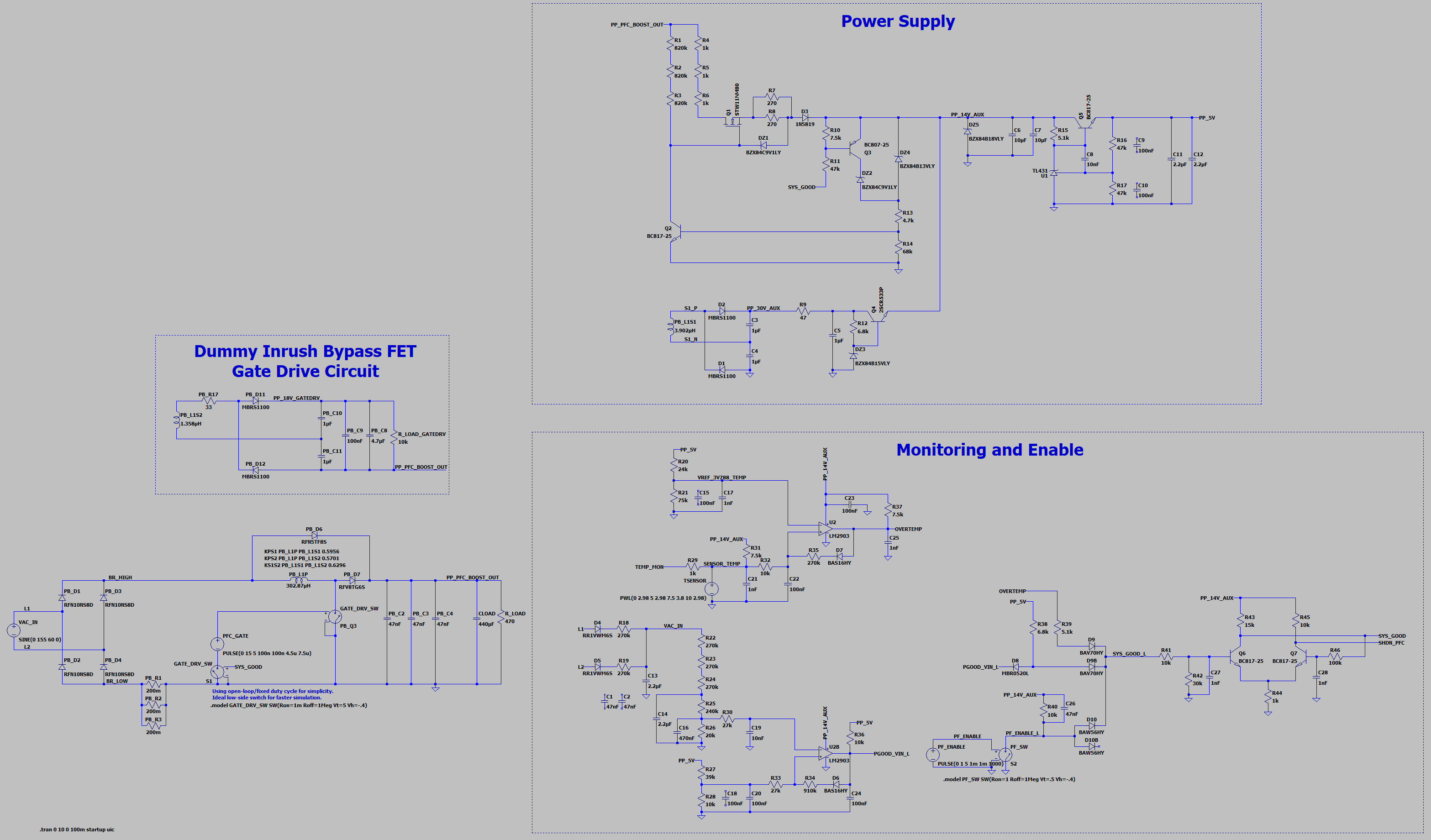
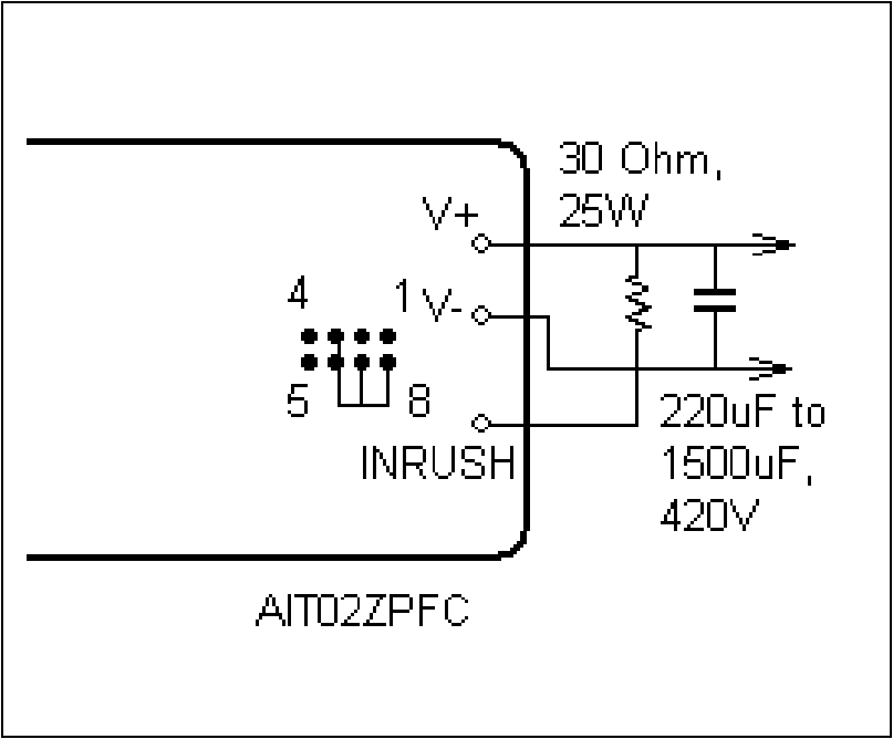
This module has provision for an inrush limiting resistor that is bypassed by an internal MOSFET once the output hold-up capacitance has been charged.
The MOSFET (Q4) is an N-channel type and thus requires a voltage at its gate that is more positive than its source in order to turn on. The gate driver circuit below is for that purpose:
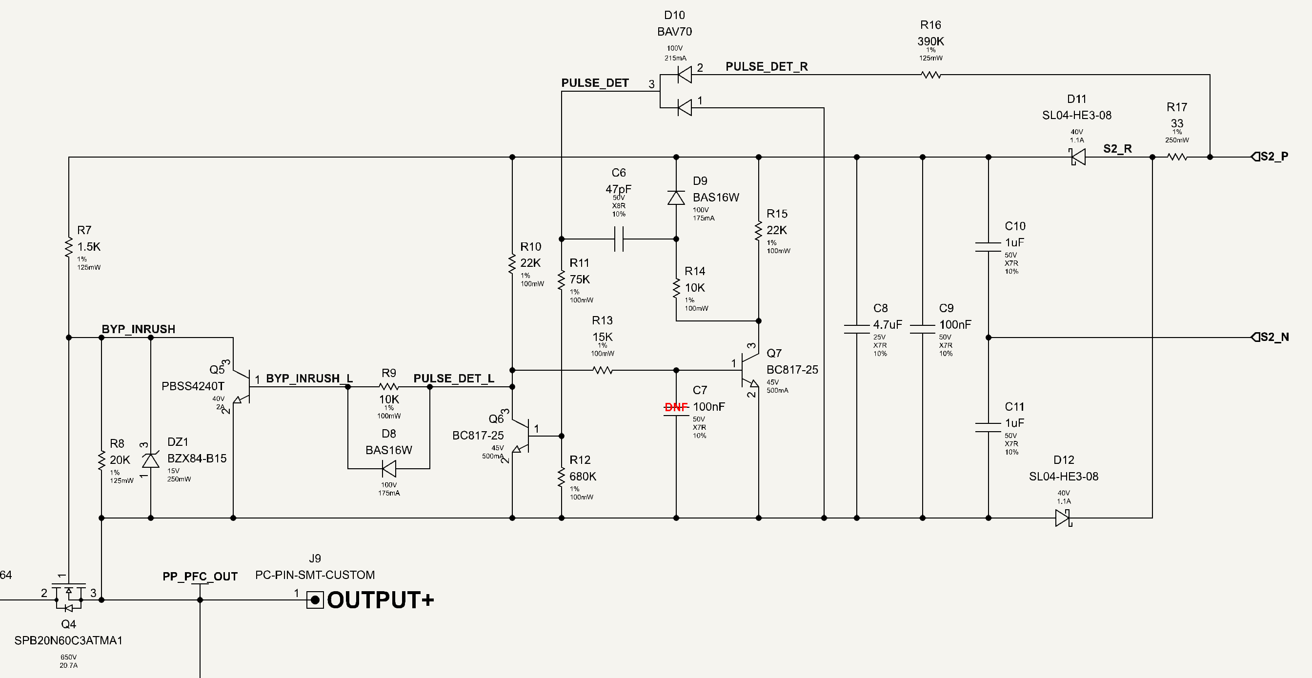
We can see this circuit floating, with its reference connected to the source of the pass MOSFET (PP_PFC_OUT). This floating gate driver is possible because of the 4-turn secondary winding we covered in the previous section. While the circuit looks complicated, we can simplify it by splitting it into a few sections.
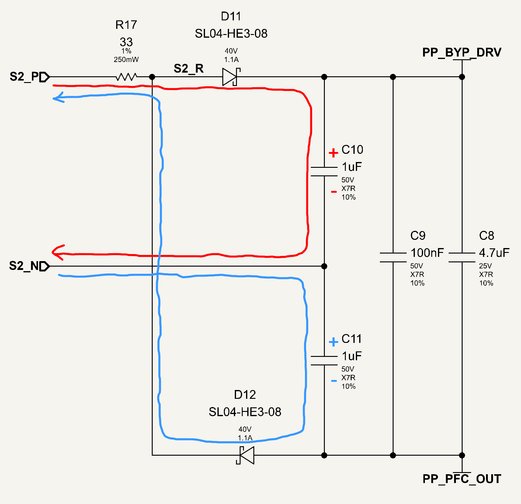
The rectifier stage shown below is a topology known as a Delon voltage multiplier. It rectifies both halves of the input waveform using two stacked peak detector circuits. The total output is naturally the sum of the voltages across C10 and C11.
Next is the block that interfaces with the gate of the pass MOSFET (Q4).
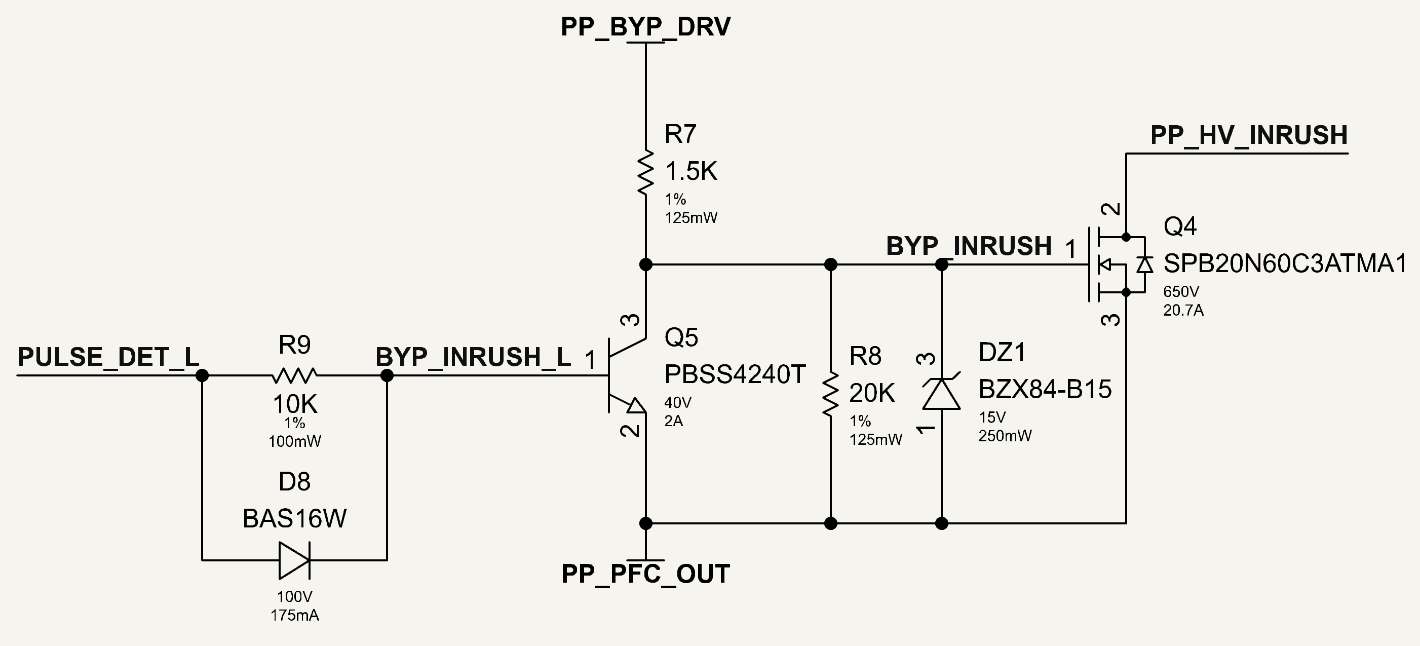
This is a basic divider that applies the lower of 15V or ~93% of PP_BYP_DRV to Q4 in order to switch it on, as long as Q5 remains off. Q5 remains off so long as PULSE_DET_L is low.
R9 and D8 are intended to provide an asymmetric turn-on rate to Q5, however in practice this would do very little to affect switching speed. This is because the input (base-emitter) capacitance for BJTs are negligible compared to the input capacitance of MOSFETs. While the PBSS4240T datasheet does not specify the input capacitance, similar NPNs like the 2N3904 and 2N2222 are in the ballpark of 20~30pF. Compare this to the input capacitance of the SPB20N60C3, which is typically 2.4nF. We can speculate that R9 and D8 may perhaps have been provisioned in the event Q5 was a MOSFET instead of a BJT.
The last section of the gate driver is the pulse detector, which monitors the AC voltage coming from the secondary winding of the boost inductor (which is also source of the PP_BYP_DRV rail), and if it drops out, disables the inrush bypass MOSFET. The bypass should only be active if the boost is working..
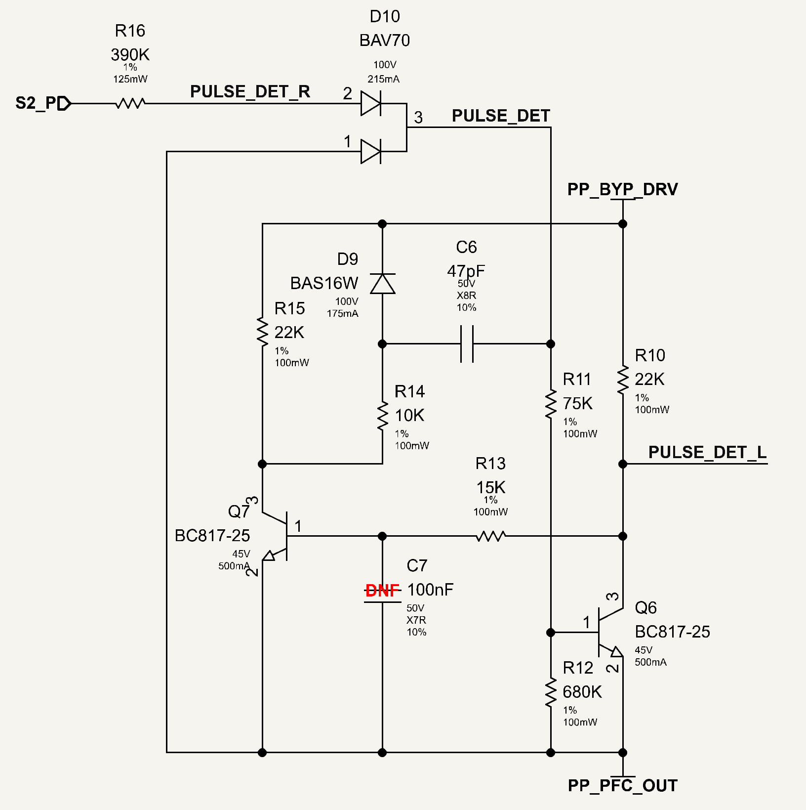
When the boost is running (AC is present at the secondary) we can see that Q6 should be off to signal (active-low) on PULSE_DET_L that a pulse is detected. The only way this can happen is if there is base current via R11 and R12, which in turn requires a voltage at PULSE_DET.
The voltage at PULSE_DET however is not DC given the half-wave rectification of S2_P by D10. Relying on this alone would result in PULSE_DET_L toggling, which in turn would toggle (PWM) the bypass FET. Therefore, C6 is added to filter out the oscillation and deliver a relatively stable base current to Q6 for the negative half-cycles of S2_P.
Given the large resistance of R16 and comparatively smaller resistance of R11 || R12, we expect the voltage on the right hand side of C6 to be small; about 15% of the peak voltage at S2_P. For example, if S2_P has a peak of 15V, we expect the right side of C6 to be ~2V after D10’s drop. The left side of C6 however will be at the potential of PP_BYP_DRV (when Q7 is off) due to the pull-up via R14 and R15. This is all to say that under normal operation (i.e. when PULSE_DET_L is low), the potential across C6 will be very close to PP_BYP_DRV; within about 2V.
When S2_P drops out, PULSE_DET becomes high-impedance, and C6 is allowed to ‘discharge’ via R11, R12, and Q6’s base toward the full potential of PP_BYP_DRV. However as it discharges, when the base current of Q6 no longer becomes sufficient to keep it on, PULSE_DET_L is pulled up to PP_BYP_DRV. The new base current through R13 via the now ungrounded R10 causes Q7 to turn on. This results in the left side of C6 being grounded through R14. C6 is however still charged to the potential of PP_BYP_DRV across it, which results in a very negative potential (equal to PP_BYP_DRV) at PULSE_DET. The bottom diode of the D10 array clamps this negative voltage to ~0.7V below ground in order to prevent emitter-base breakdown for Q6 (max 5V).
D9 is clearly provided as a positive rail clamp for C6 if the left side rises above PP_BYP_DRV. However, it’s not evident how this could ever happen in any operating state of this circuit, given R16 guarantees that PULSE_DET (the right side of C6) will always be a lower potential than PP_BYP_DRV. The only exception is if PP_BYP_DRV is discharged due to a long period of AC input absence from S2, and S2 is suddenly reintroduced. In this case, PULSE_DET will become positive w.r.t. PP_BYP_DRV for a short period. However the comparatively low source impedance (R17) of the AC supply guarantees that PP_BYP_DRV will rise faster than PULSE_DET.
Lastly, it’s not clear what purpose, if any, R14 serves. Below is an LTSpice simulation (file available here) of the above circuit showing:
S2_P (AC input)
PP_BYP_DRV
PULSE_DET
PULSE_DET_L
Voltage across C6
The pulse seen at 120ms is the response to a ~500us dropout in S2.
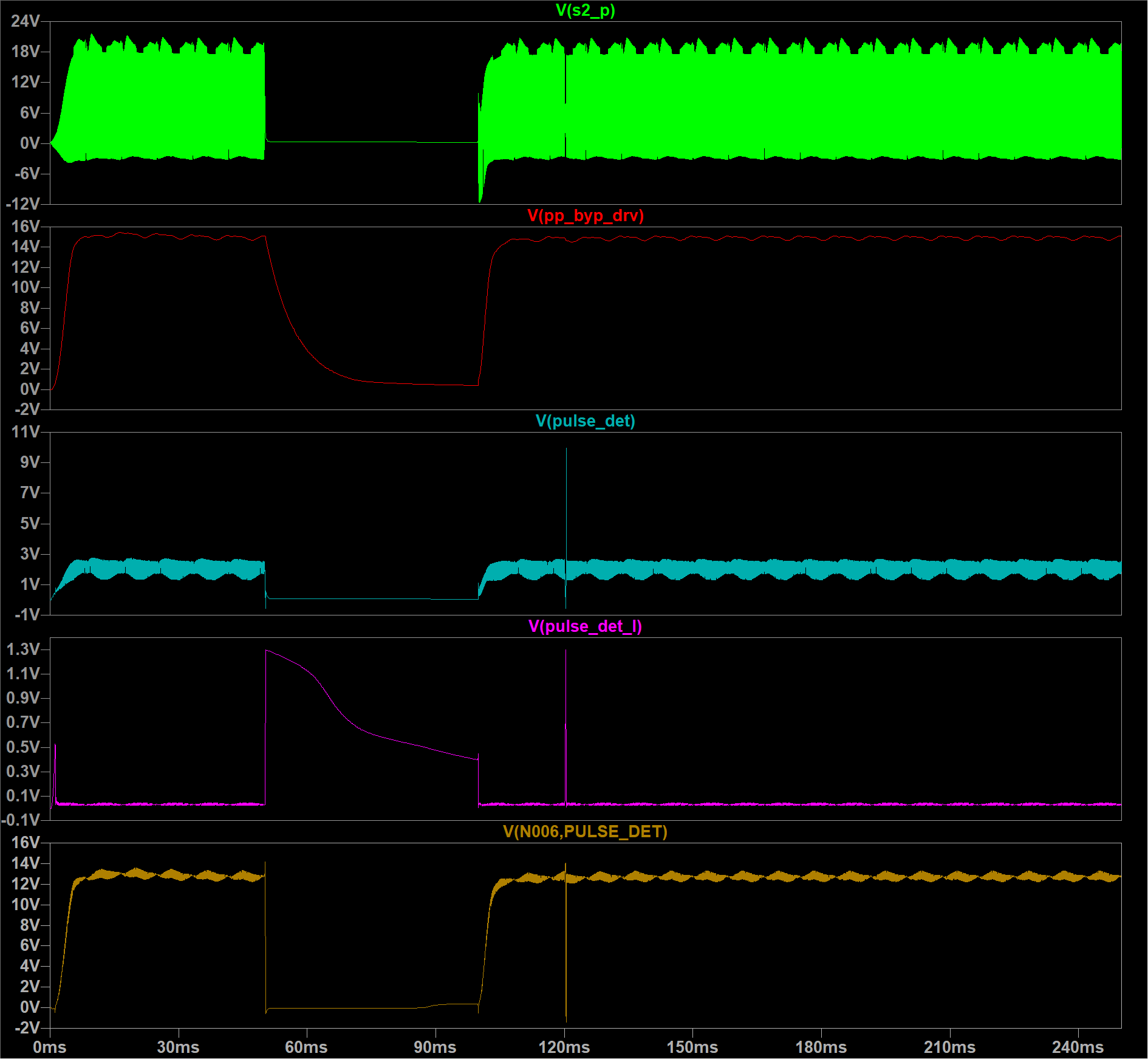
Here are the same plots with D9 removed and R14 shorted:
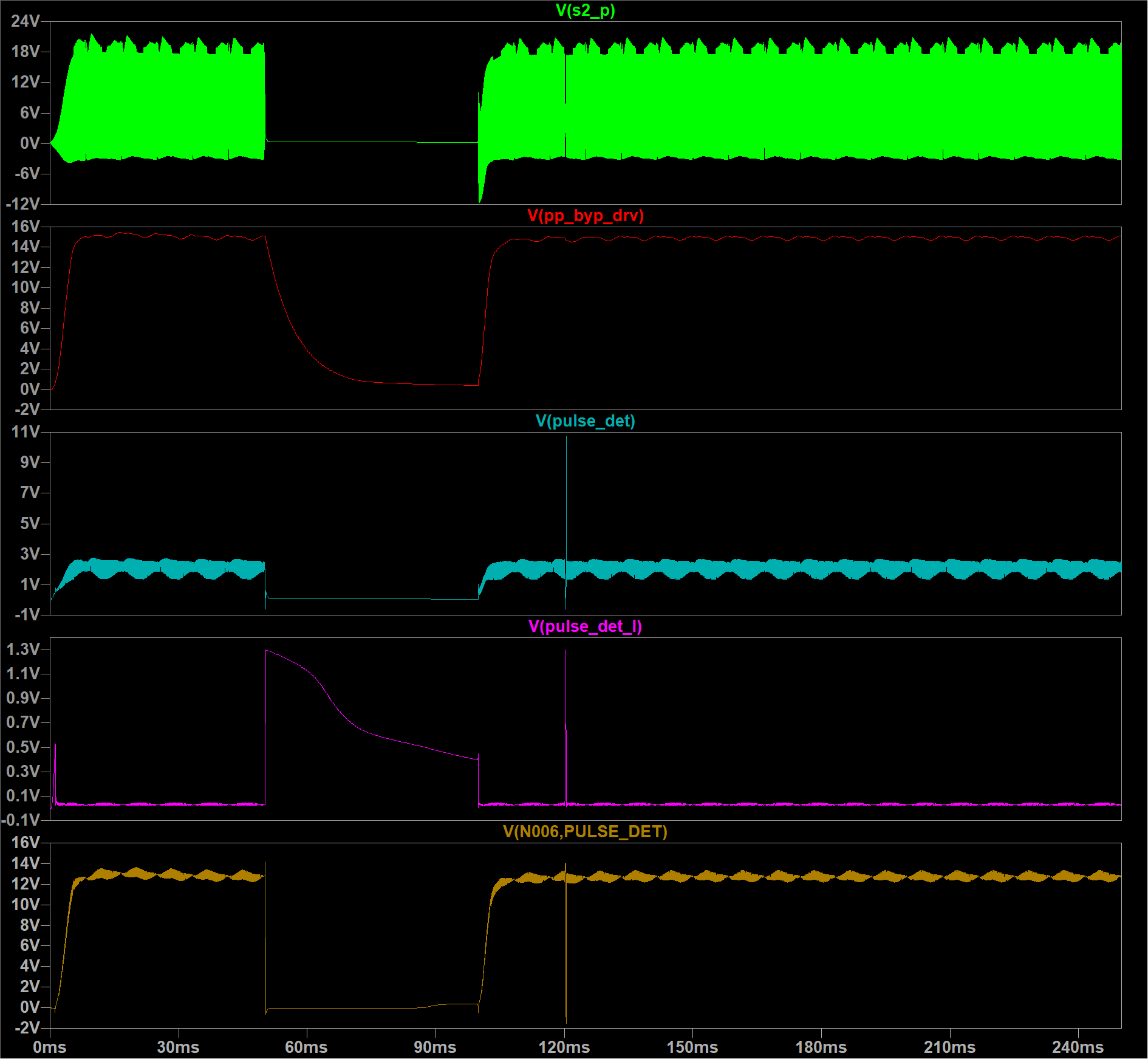
Even comparing the narrow pulse shape at the momentary interruption, the differences are negligible.
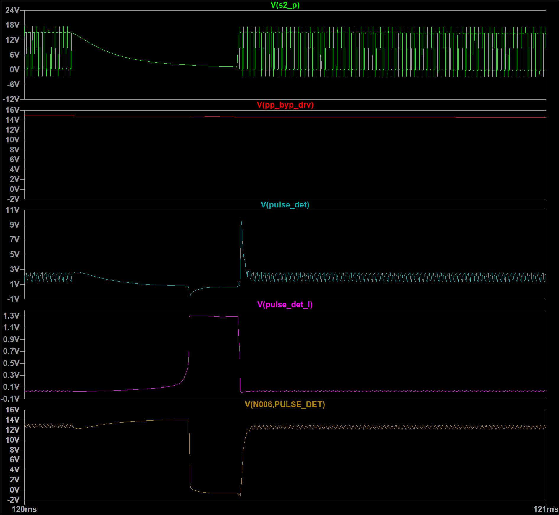
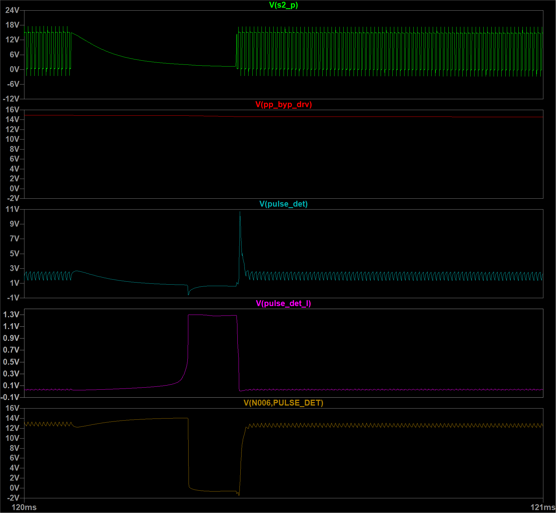
Perhaps these components serve a purpose. If they do, they’re not obvious to me based on these in-simulation tests.
The PP_14V_AUX supply is one of two power rails on the Controller board. It also powers the PFC controller and is therefore required to bootstrap the system.
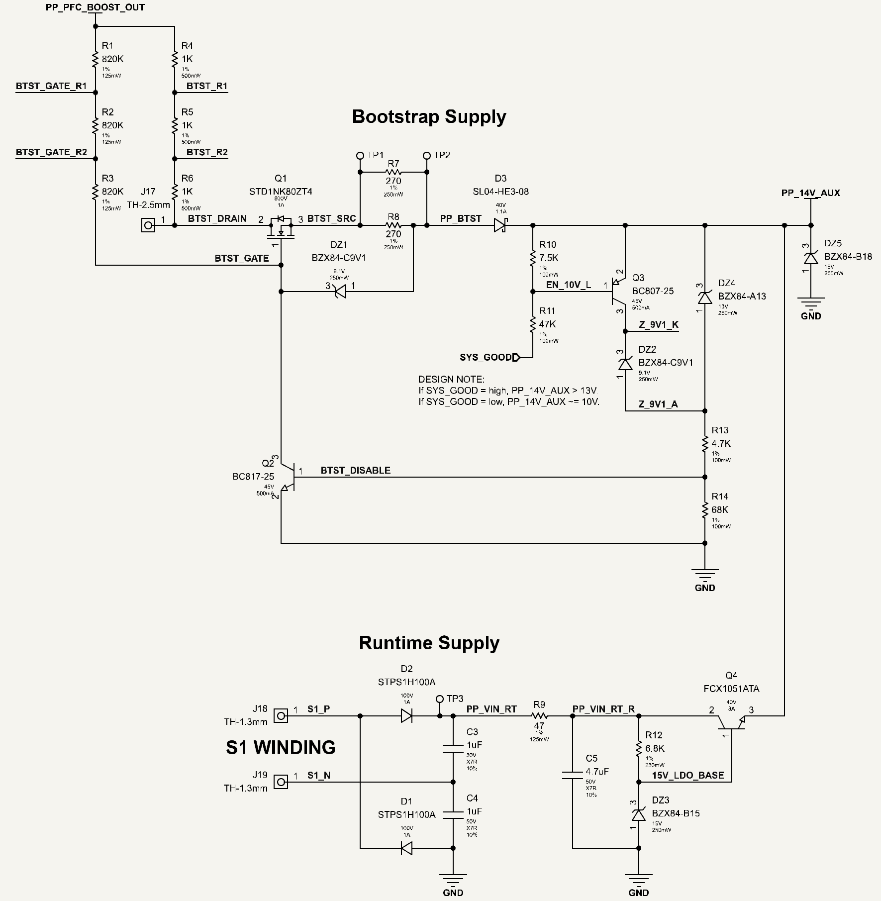
There are two sources OR’d to generate PP_14V_AUX. These two source paths have been called Bootstrap and Runtime. The Bootstrap path (per its namesake) is ‘always available’. The Runtime path by comparison is only available once the PFC controller and consequently the boost converter is running.
The Runtime supply is more efficient than the Bootstrap supply, as its source is a secondary winding comprising 7 turns on the boost’s coupled inductor, which we saw in the previous section. The turns ratio of this coupled inductor allows the Runtime supply to be much closer in potential to the final regulation point of PP_14V_AUX. This is compared to the Bootstrap supply, which must drop the rectified mains voltage (anywhere from 120V to 373V) over a chain of resistors (R4, R5, R6, R7, R8) and a series MOSFET (Q1).
To facilitate arbitration/prioritisation the Bootstrap path regulates to a lower voltage than the Runtime supply. This way, when the Runtime supply comes up, its higher voltage will allow it to have priority. The regulation point of the Bootstrap supply is determined by the 9.1V Zener (DZ2) plus a small ground offset of ~0.7V due to Q2’s VBE. Along with a small VCE offset from Q3, the Bootstrap path should loosely regulate to around 10V. This is of course, provided that SYS_GOOD is deasserted (low) and Q3 is on, as would be the case at start-up when the PFC is yet to start running. If SYS_GOOD is asserted (high), DZ4 will set the regulation point (about 13.7V), but only momentarily as the assertion of SYS_GOOD will be quickly followed by the Runtime supply coming up.
The Runtime supply’s regulation point is set by the 15V Zener (DZ3) minus a drop of ~0.7V due to Q4’s VBE. The Runtime path should thus loosely regulate to around 14.3V. This higher voltage steers addition base current into Q2 via a now strongly in breakdown DZ4. With Q2 in conduction, Q1’s gate is grounded, disconnecting the Bootstrap path and allowing the Runtime supply to fully take over as the source for PP_14V_AUX.
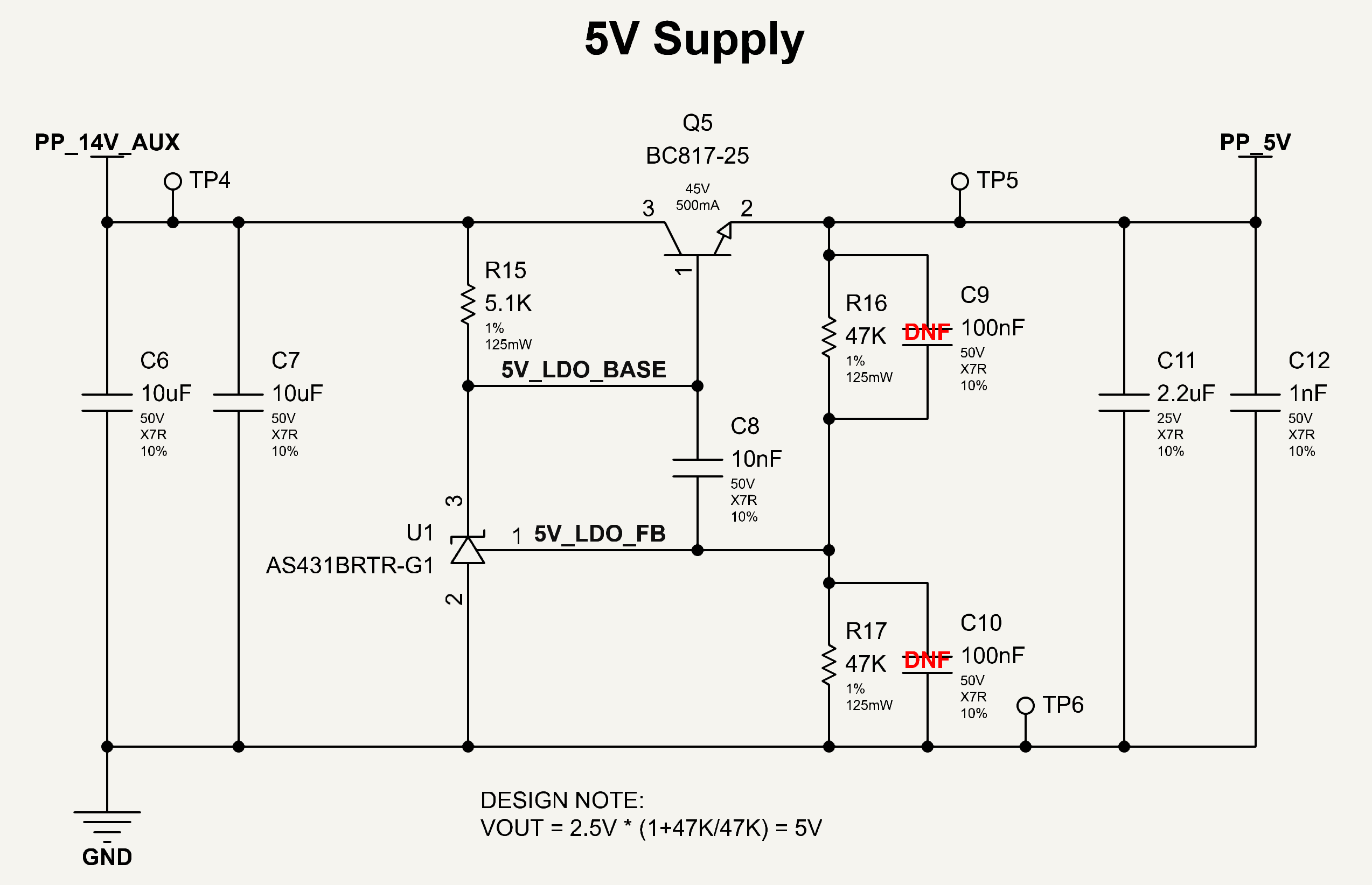
The 5V supply is used only for powering reference dividers for the monitoring circuits (Overtemperature, VIN PGOOD, Load Enable) and a handful of logic-level pull ups. Its parent supply is PP_14V_AUX.
The circuit is a very straightforward pass-transistor linear regulator that uses a TL431 as a reference. The output voltage is given by the equation:
\(V_{OUT} = 2.5\text{V}\left(1+\dfrac{R_{17}}{R_{16}}\right)\)
There are three comparator circuits for monitoring various aspects of the system:
Input voltage (RMS)
Baseplate temperature
Boost output voltage
Load enable
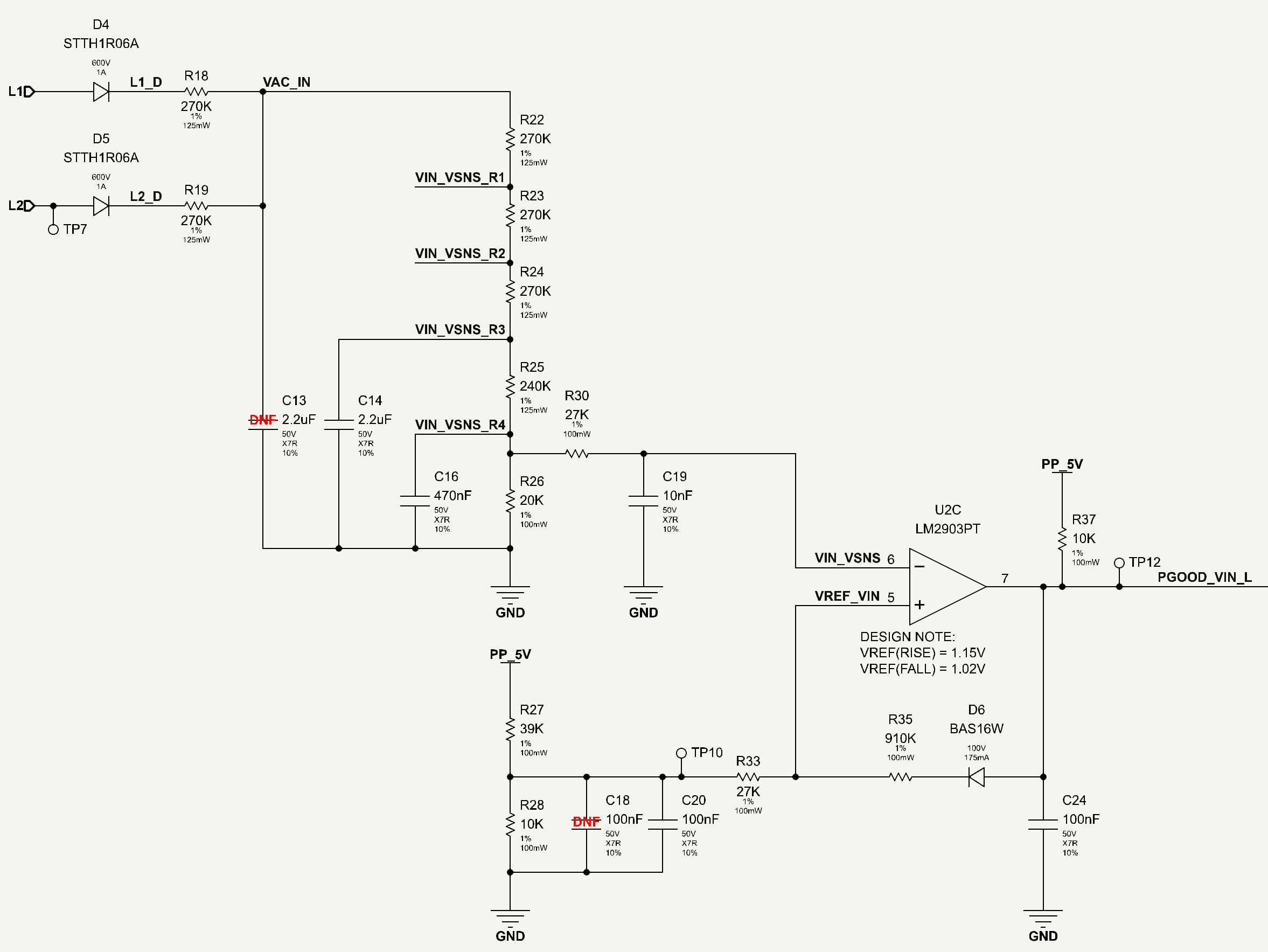
The input voltage is monitored through a resistor ladder tapped off the rectified mains input. The comparator outputs active-low when the input exceeds the reference threshold. The reference (non-inverting) input has a diode in the feedback path to add hysteresis depending on the output state of the comparator. We can calculate the potential at VREF_VIN by simplifying the feedback network into two forms; one where the comparator output is high-impedance, and another where it is driving low. Capacitors have been removed as this is a DC circuit.
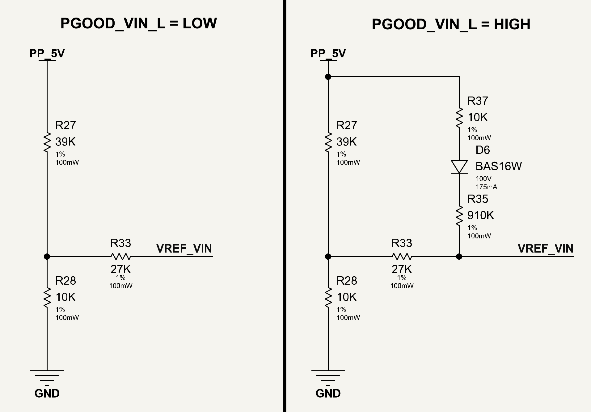
The PGOOD_VON_L = LOW case is just a basic divider (assuming negligible bias current into the comparator pin). In this state, VREF_VIN = 1.020V
We can simplify things a bit more by assuming the voltage drop across D6 will be less than 0.4V (at ~25C) given less than 5uA will be running through it.
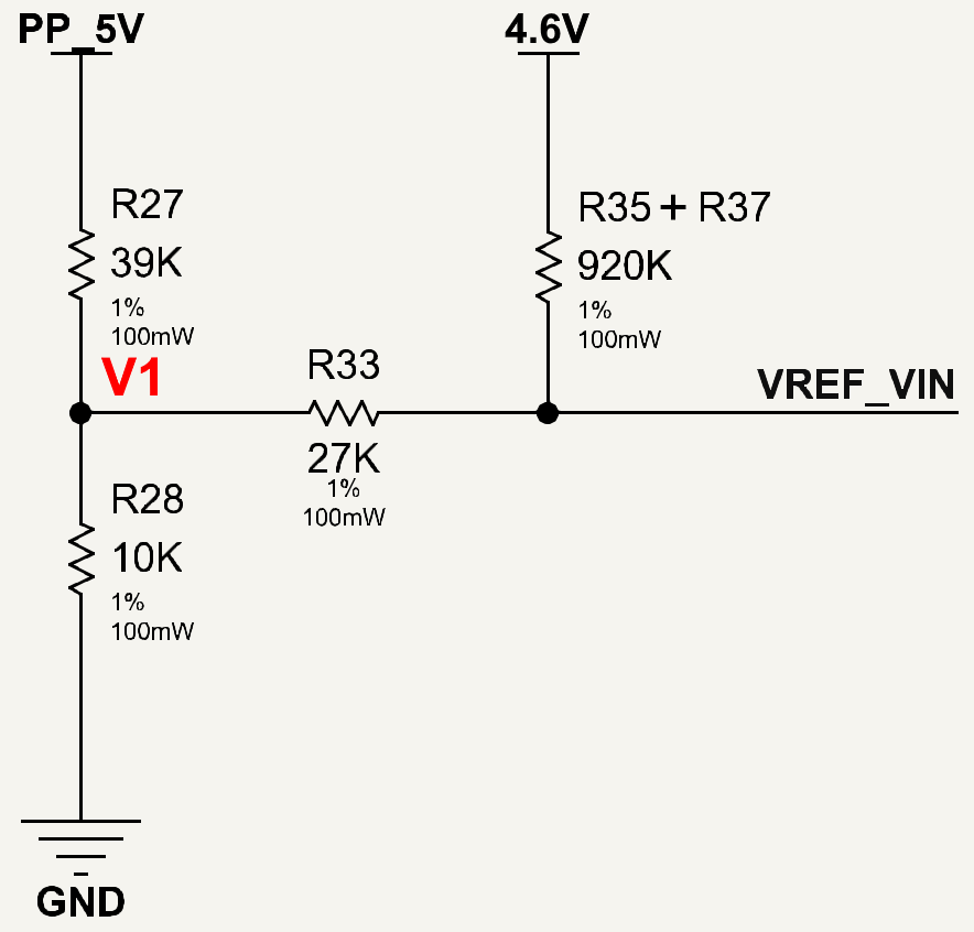
We can then write out our node equations. First obtaining an expression for V1:
\(\dfrac{5 - V_1}{R_{27}} + \dfrac{4.6 - V_1}{R_{35,37} + R_{33}}=\dfrac{V_1}{R_{28}}\)
\(\dfrac{5}{R_{27}} - \dfrac{4.6}{R_{35,37} + R_{33}} =V_1 \left(\dfrac{1}{R_{28}} + \dfrac{1}{R_{27}} + \dfrac{1}{R_{35,37} + R_{33}}\right)\)
\(\dfrac{5\left(R_{35,37} + R_{33}\right) - 4.6R_{27}}{R_{27}\left(R_{35,37} + R_{33}\right)} =V_1 \left(\dfrac{\left(R_{27}+R_{28}\right)\left(R_{35,37} + R_{33}\right) + R_{27}R_{28}}{R_{27}R_{28}\left(R_{35,37} + R_{33}\right)}\right)\)
\(V_1 = \dfrac{R_{28}\left(5\left(R_{35,37} + R_{33}\right) + 4.6R_{27}\right)}{\left(R_{27}+R_{28}\right)\left(R_{35,37} + R_{33}\right) + R_{27}R_{28}}\)
Next for VREFIN:
\(\dfrac{4.6 - V_{REFIN}}{R_{35,37}}=\dfrac{V_{REFIN} - V_1}{R_{33}}\)
\(\dfrac{V_{REFIN}}{R_{33}} + \dfrac{V_{REFIN}}{R_{35,37}}=\dfrac{4.6}{R_{35,37}} + \dfrac{V_1}{R_{33}}\)
\(\dfrac{V_{REFIN}\left(R_{35,37} + R_{33}\right)}{R_{33}R_{35,37}}=\dfrac{4.6R_{33} + V_1R_{35,37}}{R_{33}R_{35,37}}\)
\(V_{REFIN}=\dfrac{4.6R_{33}}{R_{35,37} + R_{33}}+\dfrac{ V_1R_{35,37}}{R_{35,37} + R_{33}}\)
Substituting for V1:
\(V_{REFIN}=\dfrac{4.6R_{33}}{R_{35,37} + R_{33}}+\dfrac{R_{28}R_{35,37}}{R_{35,37} + R_{33}}\left( \dfrac{5\left(R_{35,37} + R_{33}\right) + 4.6R_{27}}{\left(R_{27}+R_{28}\right)\left(R_{35,37} + R_{33}\right) + R_{27}R_{28}} \right)\)
This yields VREF_VIN = 1.151V when PGOOD_VON_L = HIGH.
Looking at the VIN side now, we can also simplify this circuit a little, though unlike the reference network, we can’t ignore the capacitors here given the presence of rectified AC at the top of the ladder.
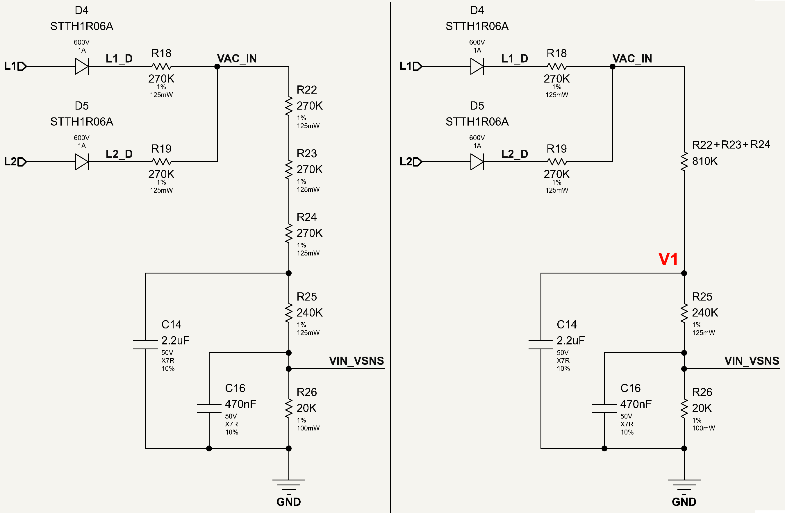
To estimate the RMS input voltage at L1/L2, we will work backward from the voltage at VIN_VSNS. This allows us to find the voltage at V1 by assuming the current through R25 and R26 are equal given negligible current into C16.
We can write our first node equation as such:
\(\dfrac{V_1 - V_{INVSNS}}{R_{25}} = \dfrac{V_{INVSNS}}{R_{26}}\)
\(V_1= V_{INVSNS}\left(\dfrac{R_{25} + R_{26}}{R_{26}}\right)\)
Next we can simplify down even further to make this look like a basic divider. I’ve only included one of R18 and R19 with the R22-R24, as only one one is active for each half cycle of the input AC waveform. Frankly, I’m not sure why they bothered to put a resistor on the output of each diode. They could have just connected the two cathodes together and put the 270k after, and the creepage/clearance would be exactly the same. But I digress.
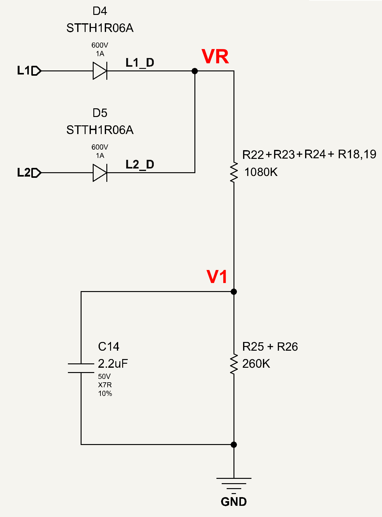
The voltage at the rectifier output VR can be expressed in terms of V1:
\(V_R = V_1\left(\dfrac{R_{25} + R_{26} + R_T}{R_{25} + R_{26}}\right)\)
Substituting in the other equation for V1:
\(V_R = V_{INVSNS}\left(\dfrac{R_{25} + R_{26}}{R_{26}}\right)\left(\dfrac{R_{25} + R_{26} + R_T}{R_{25} + R_{26}}\right)\)
\(V_R = V_{INVSNS}\left(\dfrac{R_{25} + R_{26} + R_T}{R_{26}}\right)\)
VR however is the average DC voltage. To calculate the peak AC voltage Vpk, we need:
\(V_{avg} = \dfrac{2}{\pi}V_{pk}\)
Therefore, the peak rectified voltage required for a given voltage at VIN_VSNS is:
\(V_{r-pk} = \dfrac{\pi}{2}V_{INVSNS}\left(\dfrac{R_{25} + R_{26} + R_T}{R_{26}}\right)\)
We do also have two diode drops in the bridge rectifier per half cycle that need to be accounted for:
\(V_{ac-pk} = \dfrac{\pi}{2}V_{INVSNS}\left(\dfrac{R_{25} + R_{26} + R_T}{R_{26}}\right) + 2V_D\)
Therefore, for our two VREF_VIN thresholds of 1.151V (rising) and 1.020V (falling), assuming ~0.4V dropped across each of the diodes, the required AC input voltages are:
VAC-RISE = 121.935V or 86.22Vrms
VAC-FALL = 108.148V or 76.47Vrms
This is actually somewhat in contradiction to the part datasheet, where they claim the operating voltage range is 85 ~ 264VAC
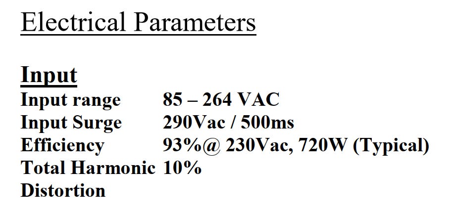
While it is true that the PFC will run at 85VAC, the input divider analysis above suggests that it must first overcome the 86.22VAC threshold before it is permitted to fall to 85VAC. Based on this, the enable threshold quoted in the datasheet is also slightly wrong (82VAC vs. 86.22VAC). The UVLO threshold is much closer (77VAC vs. 76.47VAC).

Thus if you’re designing this PFC into a system, it’s probably wise to add a bit of margin at the low end.
The temperature of the PFC’s baseplate is monitored through an LM235D PTC Zener shunt located on the Power Board. This shunt is connected across J20 and J21 on the Controller Board.
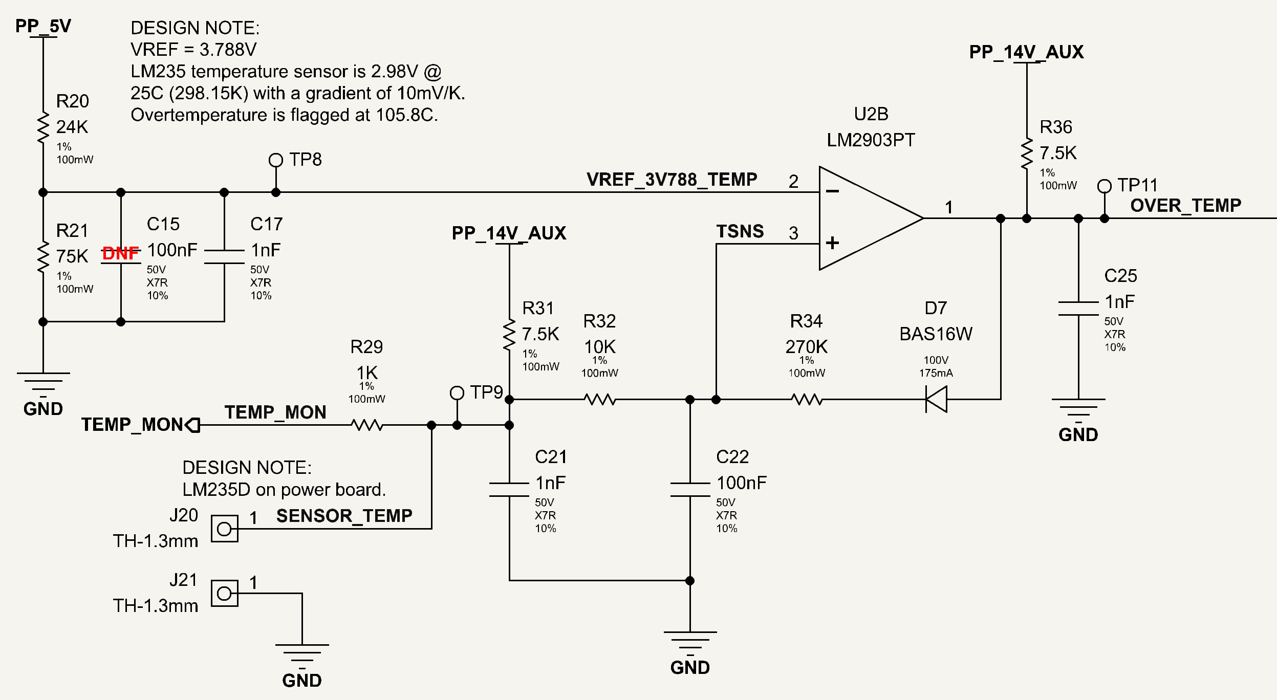
Unlike the input voltage monitor, the over-temperature comparator circuit applies hysteresis to the incoming sensor voltage rather than the reference at the inverting terminal. Thus, the reference is fixed at 3.788V.
The LM235D outputs the temperature in Kelvin with a gain of 10mV/K. This is delivered into the non-inverting input of the comparator and forms a divider with the feedback and pull-up network at the comparator’s output. The additional detail to take note of here is that the comparator output is pulled up to PP_14V_AUX. As discussed in the Bootstrap Supply section, this rail’s voltage varies depending on the state of the system, and the OVER_TEMP signal is able to influence this voltage. Thus, the potential of PP_14V_AUX determines the hysteresis of this comparator.
As before, we can draw a simplified version of the circuit seen at the non-inverting input.
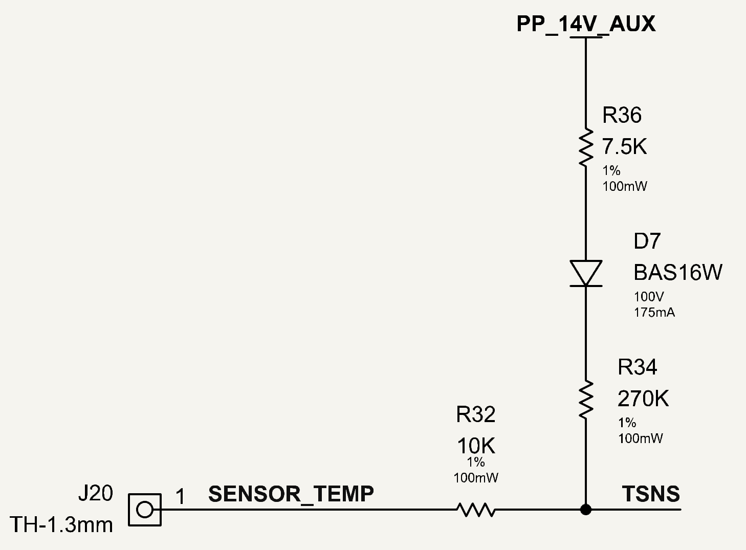
We again (due to hysteresis) have two cases depending on the state of OVER_TEMP. When OVER_TEMP is low, D7 is reverse-biased, so the comparator only sees the LM235D at SENSOR_TEMP through a 10K resistor. In other words the rising threshold for OVER_TEMP asserting is 3.788V at the LM235D, or 378.8K (105.8C).
When OVER_TEMP is high, the comparator input (TSNS) gains an additional pull-up through D7’s path. This forms a voltage divider with R32 expressed by:
\(\dfrac{V_{AUX} - V_{TSNS}-V_D}{R_{34} + R_{36}} = \dfrac{V_{TSNS}-V_{SENSOR}}{R_{32}}\)
\(V_{TSNS}\left(\dfrac{R_{32} + R_{34} + R_{36}}{R_{32}\left(R_{34} + R_{36}\right)}\right) = \dfrac{R_{32}\left(V_{AUX} -V_D\right) + V_{SENSOR}\left(R_{34} + R_{36}\right)}{R_{32}\left(R_{34} + R_{36}\right)}\)
\(V_{TSNS} = \dfrac{R_{32}\left(V_{AUX} -V_D\right) + V_{SENSOR}\left(R_{34} + R_{36}\right)}{R_{32} + R_{34} + R_{36}}\)
Alternatively, we can also rearrange this to solve for the voltage at the LM235D:
\(V_{SENSOR} = \dfrac{V_{TSNS}\left(R_{32} + R_{34} + R_{36}\right) - R_{32}\left(V_{AUX} -V_D\right)}{R_{34} + R_{36}}\)
If we assume VD is approximately 0.4V and VAUX is ~10V when OVER_TEMP is asserted; given VTSNS needs to be 3.788V or less for OVER_TEMP to deassert, the LM235D output needs to fall to at most 3.578V, which is 357.8K (84.8C).
Once again however, there are discrepancies between the analysis and the thresholds claimed in the datasheet.
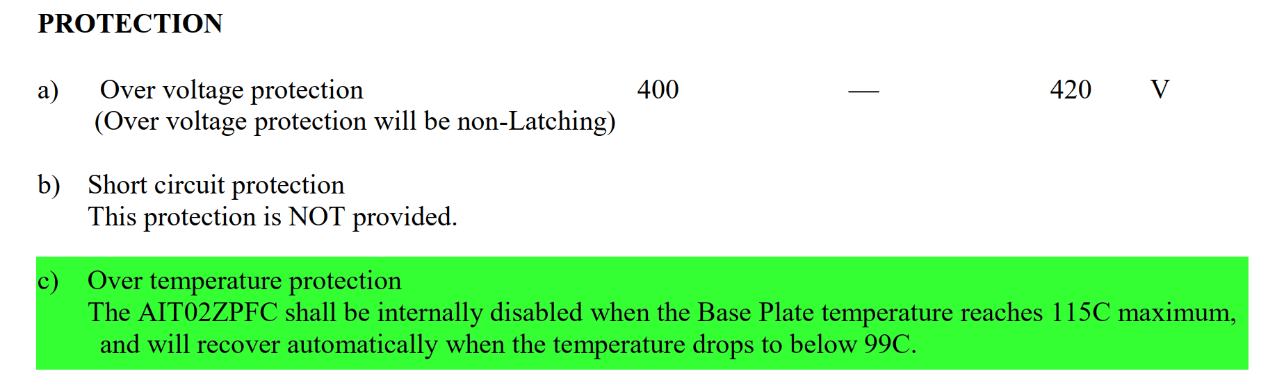
It’s possible that the datasheet is factoring for delta (thermal resistance) between the baseplate and the LM235D die. However if so, the delta is larger at 99C than it is at 115C (14.2C vs. 9.2C), whereas one would expect it to be fixed.
There are two parts to the boost output monitoring circuit; the feedback network into the PFC controller, and the PFC PGOOD comparator. We will start with the latter.
The PGOOD circuit is a basic comparator without hysteresis. The reference voltage is fixed at 1.135V and is compared against the voltage at PGOOD_PFC_VSNS.
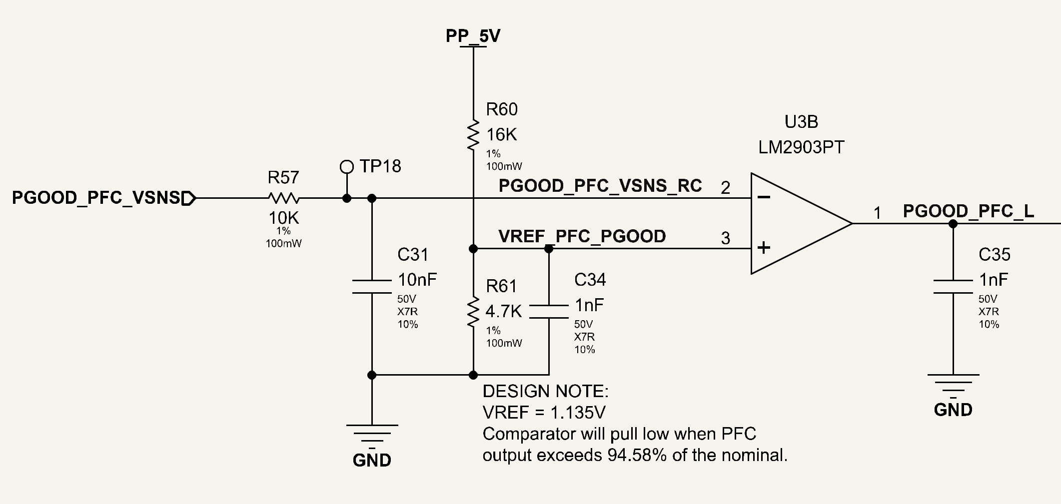
PGOOD_PFC_VSNS itself is a divider off the feedback pin of the PFC controller PFC_VSENSE_3V. When the PFC is in regulation, PFC_VSENSE_3V will always be at 3V, and in turn, PGOOD_PFC_VSNS will be at 1.2V
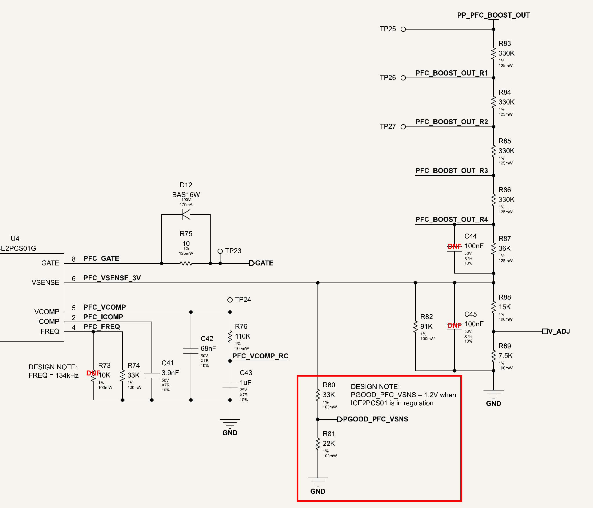
This means that the PFC PGOOD comparator will assert when the boost output is within 94.58% of its target voltage.
The output voltage itself is adjustable through the V_ADJ pin on the module. We can simplify the feedback network as follows:
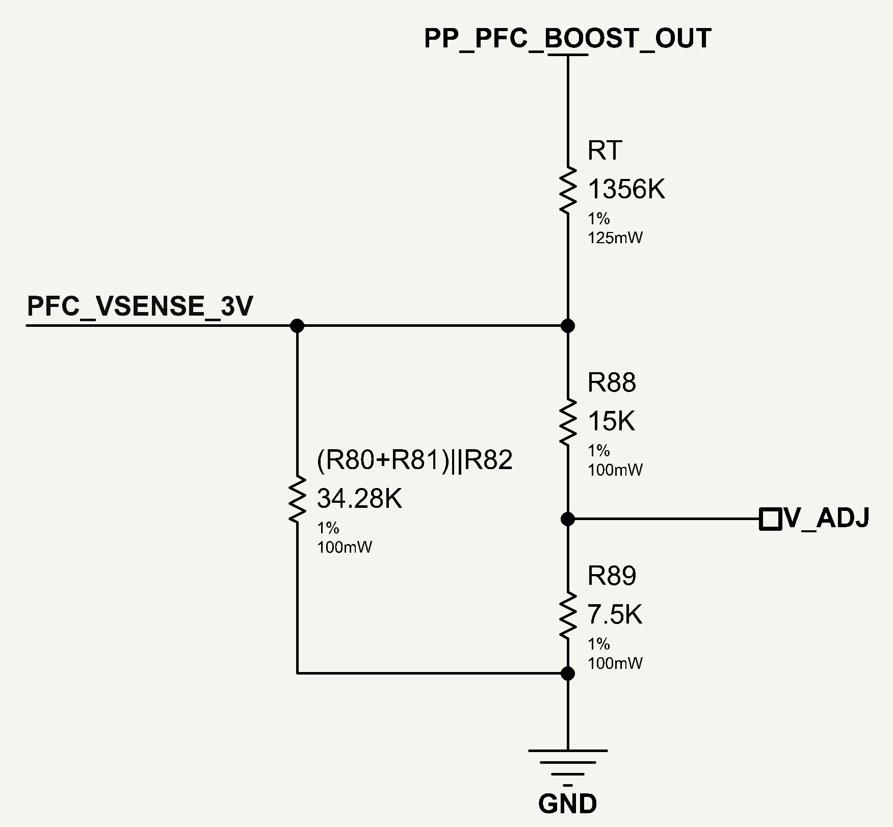
The datasheet provides the following equation for calculating the output voltage:
\(V_{OUT} = V_R\left(1+\dfrac{R_h}{R_2+\dfrac{1}{\dfrac{1}{R_3 + R}+\dfrac{1}{R_1}}}\right)\)
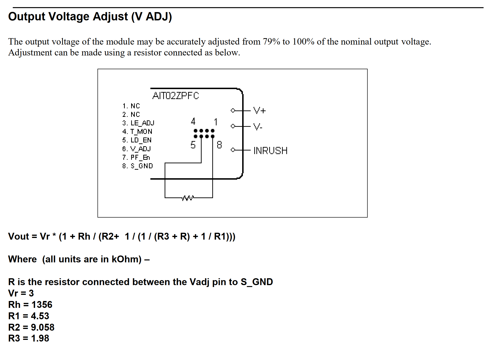
Here is what that equation looks like in schematic form:
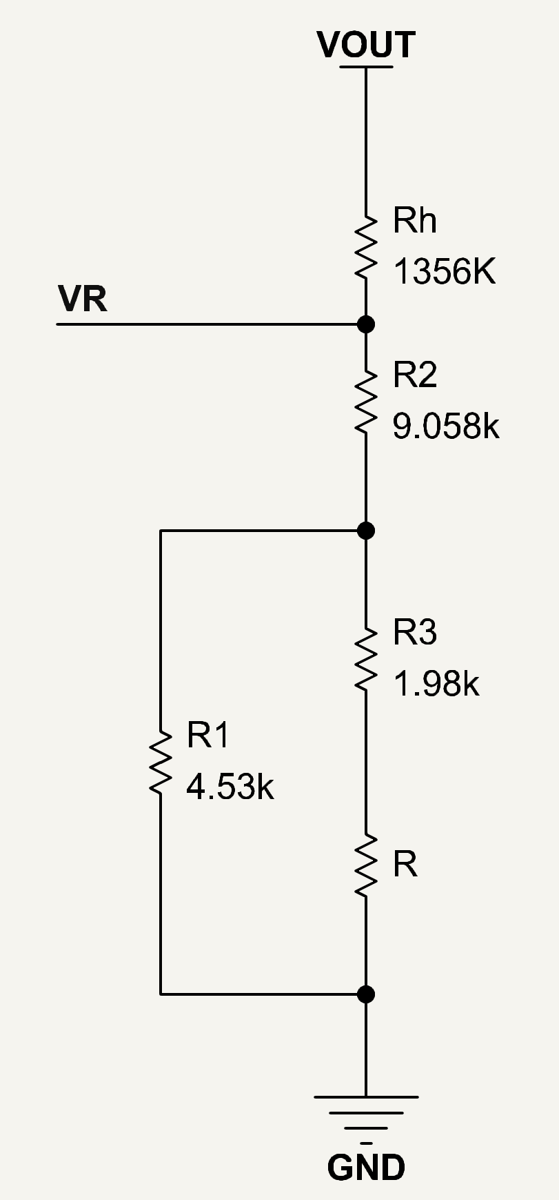
This looks quite different from the physical circuit on the board. We can see the lumped 1356K resistor chain is the same, but the network below the regulation point VR is nothing alike. These circuits are however equivalent and we can demonstrate it by looking at the open circuit voltage and short circuit current at V_ADJ.
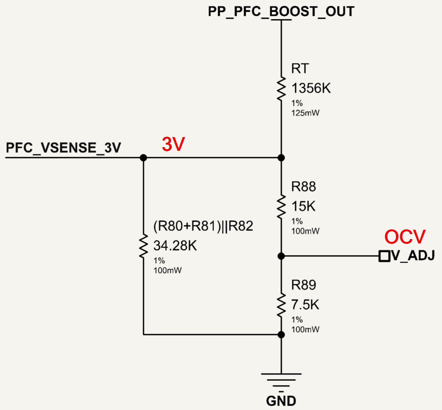
First, we can see that given PFC_VSENSE_3V (we will call this VR henceforth for compactness) must always regulate to a fixed voltage during normal operation, the OCV at V_ADJ is simply the output of the potential divider R88 and R89.
\(V_{ADJ-OCV} = V_{FB}\left(\dfrac{R_{89}}{R_{88}+R_{89}}\right)\)
Next, we can calculate equivalent resistance at the bottom half of the divider with V_ADJ open-circuit.
\(R_{B-OC} = \dfrac{1}{\dfrac{1}{R_{80}+R_{81}}+\dfrac{1}{R_{82}}+\dfrac{1}{R_{88}+R_{89}}}\)
\(R_{B-OC} =\dfrac{R_{82}\left(R_{80}+R_{81}\right)\left(R_{88}+R_{89}\right)}{R_{82}\left(R_{88}+R_{89}\right) + \left(R_{80}+R_{81}\right)\left(R_{88}+R_{89}\right) + R_{82}\left(R_{80}+R_{81}\right)}\)
We can now use this to solve for R1 and R2 below. We recognise that whatever the value of R1 and R2, the voltage at VADJ in open circuit must preserve the ratio of R88 and R89 in our physical circuit.
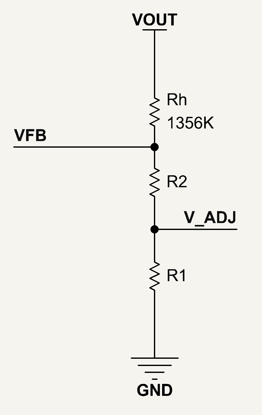
Therefore:
\(R_1 = \left(\dfrac{R_{89}}{R_{88}+R_{89}}\right)R_{B-OC}\)
\(R_1 = \dfrac{R_{82}R_{89}\left(R_{80}+R_{81}\right)}{R_{82}\left(R_{88}+R_{89}\right) + \left(R_{80}+R_{81}\right)\left(R_{88}+R_{89}\right) + R_{82}\left(R_{80}+R_{81}\right)}\)
Naturally, R2 is simply:
\(R_2 = R_{B-OC}-R_1\)
\(R_2 = \dfrac{R_{82}\left(R_{80}+R_{81}\right)\left(R_{88}+R_{89}\right)-R_{82}R_{89}\left(R_{80}+R_{81}\right)}{R_{82}\left(R_{88}+R_{89}\right) + \left(R_{80}+R_{81}\right)\left(R_{88}+R_{89}\right) + R_{82}\left(R_{80}+R_{81}\right)}\)
\(R_2 = \dfrac{R_{82}R_{88}\left(R_{80}+R_{81}\right)}{R_{82}\left(R_{88}+R_{89}\right) + \left(R_{80}+R_{81}\right)\left(R_{88}+R_{89}\right) + R_{82}\left(R_{80}+R_{81}\right)}\)
We will now solve for the last element, R3 in series with V_ADJ
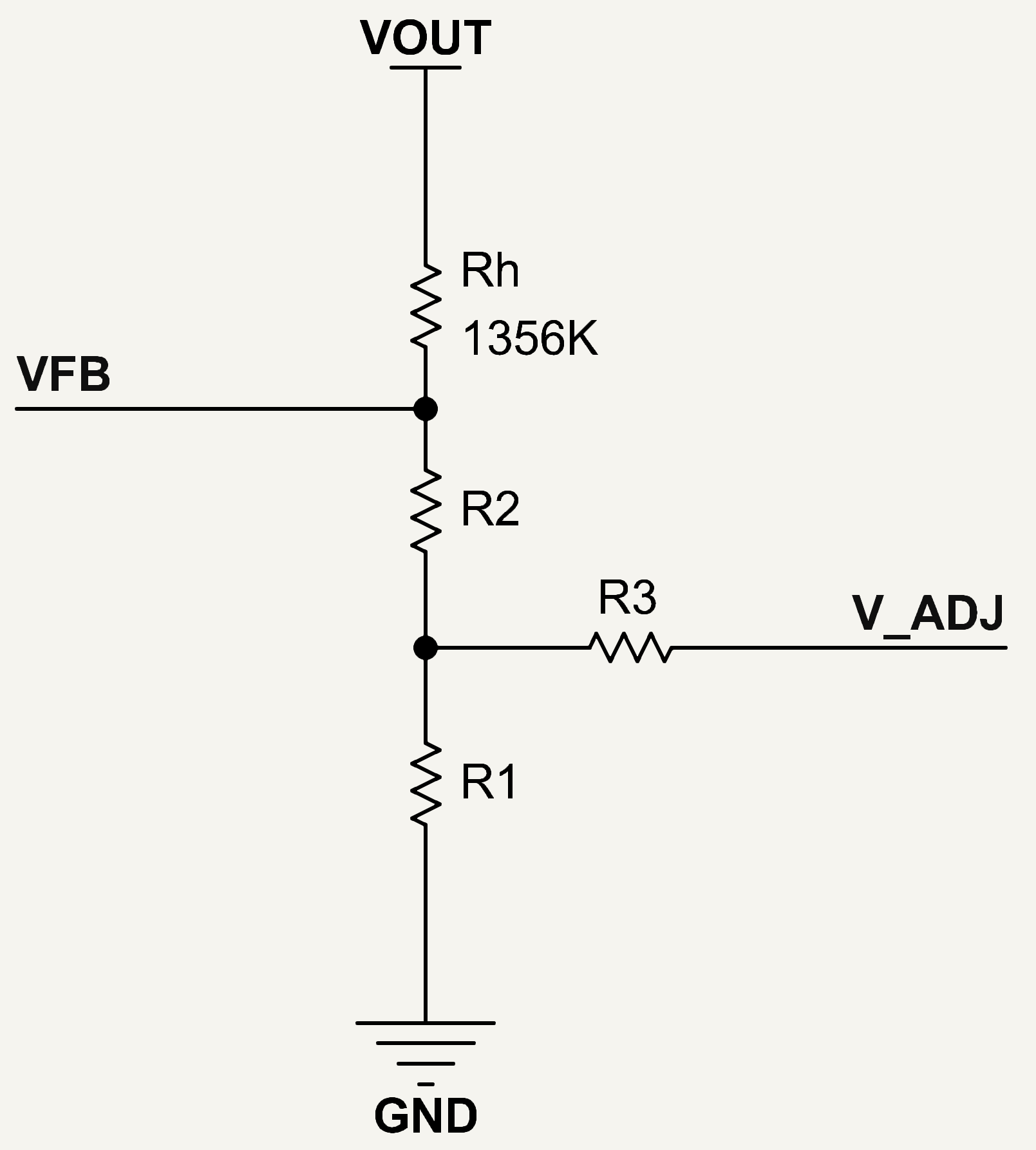
In our physical circuit, the short circuit current for V_ADJ is:
\(I_{ADJ-SC} = \dfrac{V_{FB}}{R_{88}}\)
The equivalent resistance of the lower half of the divider when V_ADJ is shorted is:
\(R_{B-SC} = \dfrac{1}{\dfrac{1}{R_{80}+R_{81}}+\dfrac{1}{R_{82}}+\dfrac{1}{R_{88}}}\)
\(R_{B-SC} = \dfrac{R_{82}R_{88}\left(R_{80}+R_{81}\right)}{R_{82}R_{88} + R_{82}\left(R_{80}+R_{81}\right)+R_{88}\left(R_{80}+R_{81}\right)}\)
When V_ADJ is shorted to ground, R3 becomes paralleled with R1. We know that whatever the resistance of R3, the equivalent resistance of the circuit comprising R1, R2, and R3 must be equal to RB-SC.
\(R_2 + \dfrac{1}{\dfrac{1}{R_1}+\dfrac{1}{R_3}} = R_{B-SC}\)
\(\dfrac{1}{R_{B-SC}-R_2} = \dfrac{1}{R_1}+\dfrac{1}{R_3}\)
\(R_3 = \dfrac{R_1\left(R_{B-SC}-R_2\right)}{R_1 + R2 - R_{B-SC}}\)
Substituting the resistances, we get the following:
R1 = 4.528K
R2 = 9.056K
R3 = 1.981K
These of course match those in the datasheet almost exactly.
The load enable monitor signals to external circuits that the PFC has started up and is ready to accept downstream loads. It does so by monitoring the output of the boost after the inrush resistor bypass MOSFET to determine whether the external holdup capacitors have sufficiently charged.
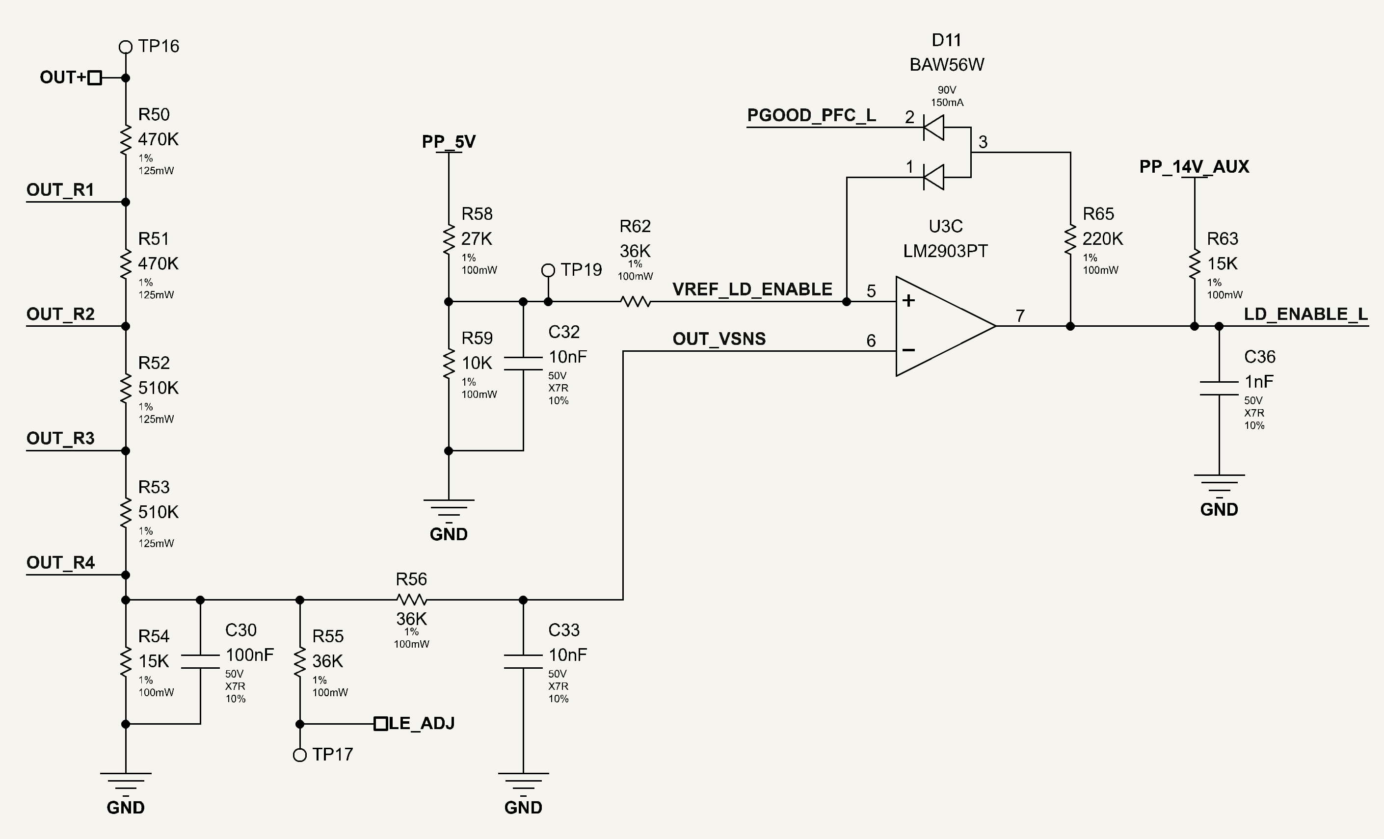
This comparator also has hysteresis whose configuration is a mixture between the input voltage and baseplate temperature monitor circuits. That is, like the input voltage monitor, the hysteresis is applied to the reference divider, and like the temperature monitor, the output is pulled up to the variable PP_14V_AUX rail.
The network can be simplified as follows:
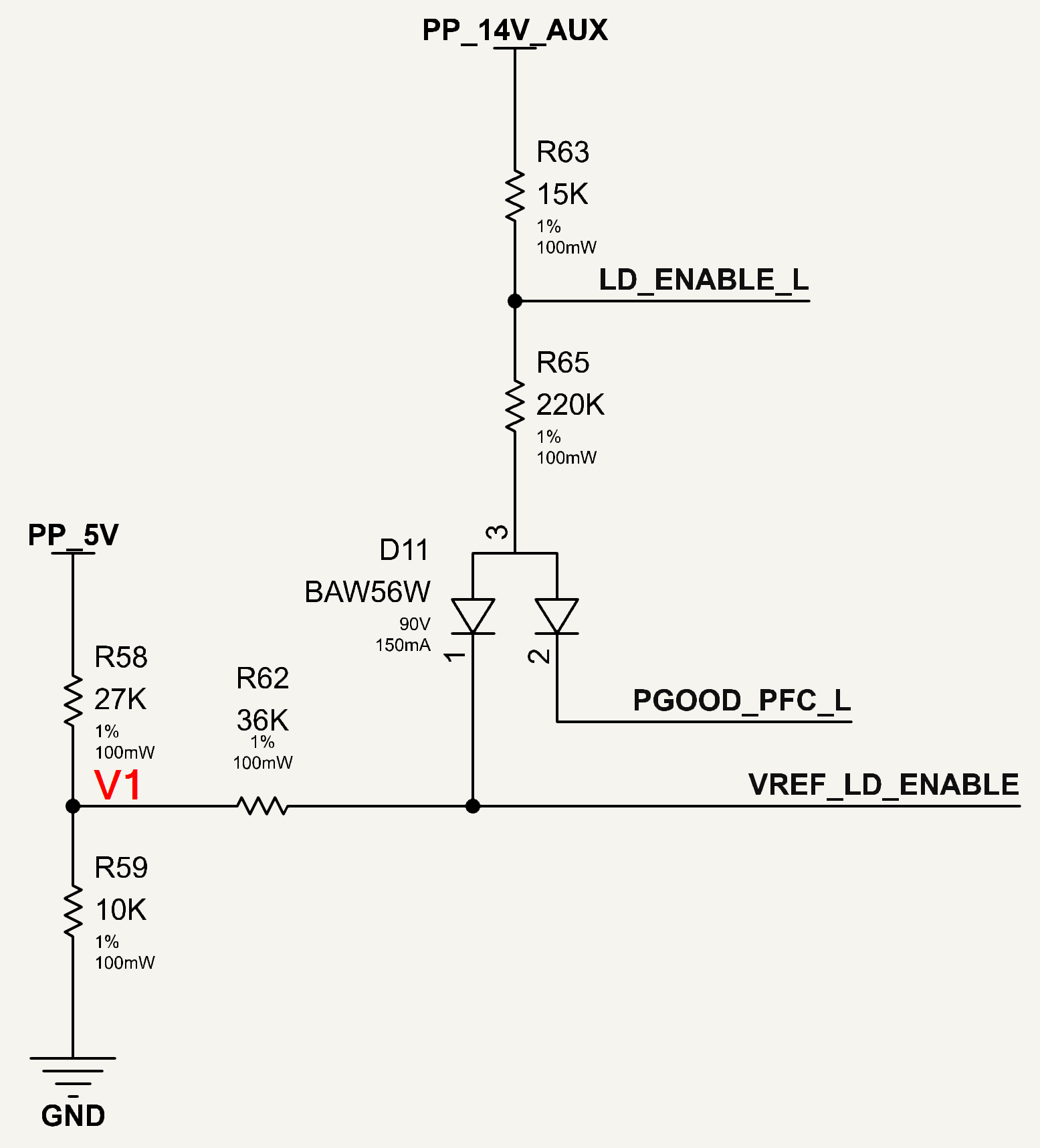
When either LD_ENABLE_L or PGOOD_PFC_L are asserted (low), D11’s connection to VREF_LD_ENABLE is reverse-biased. The voltage at VREF_LD_ENABLE in this state is just determined by the basic R58-R59 divider. So when either LD_ENABLE_L or PGOOD_PFC_L are asserted, the threshold to meet or exceed is:
\(V_{REF\_LDE} = 5\text{V}\dfrac{R_{59}}{R_{58}+R_{59}} = 1.351\text{V}\)
When both LD_ENABLE_L and PGOOD_PFC_L deasserted, there is an additional pull-up to PP_14V_AUX through R63, R65 and D11. The node equations in this state are as follows:
\(\dfrac{V_{AUX} - V_D - V_{REF\_LDE}}{R_{63}+R_{65}} = \dfrac{V_{REF\_LDE} - V_1}{R_{62}}\)
\(\dfrac{V_{AUX} - V_D}{R_{63}+R_{65}} + \dfrac{V_1}{R_{62}} = \dfrac{V_{REF\_LDE}}{R_{62}} + \dfrac{V_{REF\_LDE}}{R_{63}+R_{65}}\)
\(\dfrac{R_{62}\left(V_{AUX} - V_D\right) + V_1\left(R_{63}+R_{65}\right)}{R_{62}\left(R_{63}+R_{65}\right)} = \dfrac{V_{REF\_LDE}\left(R_{62}+R_{63}+R_{65}\right)}{R_{62}\left(R_{63}+R_{65}\right)}\)
\(V_{REF\_LDE} = \dfrac{R_{62}\left(V_{AUX} - V_D\right) + V_1\left(R_{63}+R_{65}\right)}{R_{62}+R_{63}+R_{65}}\)
Next the PP_5V divider:
\(\dfrac{V_{5V} - V_1}{R_{58}} + \dfrac{V_{REF\_LDE} - V_1}{R_{62}}= \dfrac{V_1}{R_{59}}\)
\(\dfrac{V_{5V}}{R_{58}} + \dfrac{V_{REF\_LDE}}{R_{62}}= \dfrac{V_1}{R_{58}} + \dfrac{V_1}{R_{59}} + \dfrac{V_1}{R_{62}}\)
\(\dfrac{V_{5V}R_{62} + V_{REF\_LDE}R_{58}}{R_{58}R_{62}} = V_1\left(\dfrac{R_{59}R_{62} + R_{58}R_{62} + R_{58}R_{59}}{R_{58}R_{59}R_{62}}\right)\)
\(V_1 = \dfrac{R_{59}\left(V_{5V}R_{62} + V_{REF\_LDE}R_{58}\right)}{R_{59}R_{62} + R_{58}R_{62} + R_{58}R_{59}}\)
Substituting for V1:
\(V_{REF\_LDE} = \dfrac{R_{62}\left(V_{AUX} - V_D\right)}{R_{62}+R_{63}+R_{65}} + \left(\dfrac{R_{59}\left(V_{5V}R_{62} + V_{REF\_LDE}R_{58}\right)}{R_{59}R_{62} + R_{58}R_{62} + R_{58}R_{59}}\right)\left(\dfrac{R_{63}+R_{65}}{R_{62}+R_{63}+R_{65}}\right)\)
\(V_{REF\_LDE} = \dfrac{R_{62}\left(V_{AUX} - V_D\right)}{R_{62}+R_{63}+R_{65}} + \left(\dfrac{V_{5V}R_{59}R_{62}}{R_{59}R_{62} + R_{58}R_{62} + R_{58}R_{59}} + \dfrac{V_{REF\_LDE}R_{58}R_{59}}{R_{59}R_{62} + R_{58}R_{62} + R_{58}R_{59}}\right) \left(\dfrac{R_{63}+R_{65}}{R_{62}+R_{63}+R_{65}}\right)\)
\(V_{REF\_LDE} = \dfrac{R_{62}\left(V_{AUX} - V_D\right)}{R_{62}+R_{63}+R_{65}} + \dfrac{V_{5V}R_{59}R_{62}\left(R_{63}+R_{65}\right)}{\left(R_{62}+R_{63}+R_{65}\right)\left(R_{59}R_{62} + R_{58}R_{62} + R_{58}R_{59}\right)} + \dfrac{V_{REF\_LDE}R_{58}R_{59}\left(R_{63}+R_{65}\right)}{\left(R_{62}+R_{63}+R_{65}\right)\left(R_{59}R_{62} + R_{58}R_{62} + R_{58}R_{59}\right)} \)
\(V_{REF\_LDE}\left(1 - \dfrac{R_{58}R_{59}\left(R_{63}+R_{65}\right)}{\left(R_{62}+R_{63}+R_{65}\right)\left(R_{59}R_{62} + R_{58}R_{62} + R_{58}R_{59}\right)}\right) = \dfrac{R_{62}\left(V_{AUX} - V_D\right)}{R_{62}+R_{63}+R_{65}} + \dfrac{V_{5V}R_{59}R_{62}\left(R_{63}+R_{65}\right)}{\left(R_{62}+R_{63}+R_{65}\right)\left(R_{59}R_{62} + R_{58}R_{62} + R_{58}R_{59}\right)} \)
\(V_{REF\_LDE}\left(\dfrac{\left(R_{62}+R_{63}+R_{65}\right)\left(R_{59}R_{62} + R_{58}R_{62} + R_{58}R_{59}\right) - R_{58}R_{59}\left(R_{63}+R_{65}\right)}{R_{59}R_{62} + R_{58}R_{62} + R_{58}R_{59}}\right) = R_{62}\left(V_{AUX} - V_D\right)+ \dfrac{V_{5V}R_{59}R_{62}\left(R_{63}+R_{65}\right)}{R_{59}R_{62} + R_{58}R_{62} + R_{58}R_{59}} \)
\(V_{REF\_LDE} = \dfrac{R_{62}\left(V_{AUX} - V_D\right)\left(R_{59}R_{62} + R_{58}R_{62} + R_{58}R_{59}\right)+ V_{5V}R_{59}R_{62}\left(R_{63}+R_{65}\right)} {\left(R_{62}+R_{63}+R_{65}\right)\left(R_{59}R_{62} + R_{58}R_{62} + R_{58}R_{59}\right) - R_{58}R_{59}\left(R_{63}+R_{65}\right)}\)
\(V_{REF\_LDE} = \dfrac{\left(V_{AUX} - V_D\right)\left(R_{59}R_{62} + R_{58}R_{62} + R_{58}R_{59}\right)+ V_{5V}R_{59}\left(R_{63}+R_{65}\right)} {R_{62}\left(R_{58}+R_{59}\right)+R_{58}\left(R_{59} + R_{63} + R_{65}\right)+R_{59}\left(R_{63}+R_{65}\right)}\)
Assuming a 0.4V diode drop, and ~10V at PP_14V_AUX (as would be the case if the PFC is disabled intentionally or due to a fault), VREF_LD_ENABLE will be 2.635V.
On the output voltage sense ladder, similar to the output voltage, we have adjustability via the LE_ADJ pin.
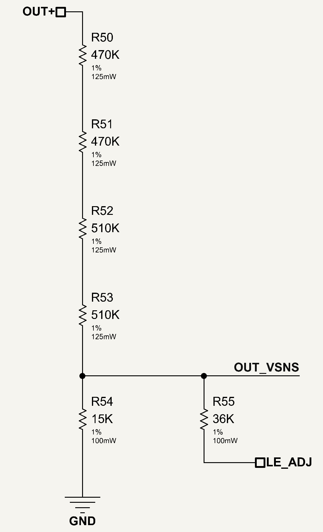
The equations below calculate the output voltage for a given voltage at the comparator input for both short and open cases of LE_ADJ:
Open Circuit
\(V_{OUT} = V_{SNS}\left(\dfrac{R_{50}+R_{51}+R_{52}+R_{53}}{R_{54}} + 1\right)\)
Short Circuit
\(V_{OUT} = V_{SNS}\left(\left(R_{50}+R_{51}+R_{52}+R_{53}\right)\left(\dfrac{1}{R_{54}}+ \dfrac{1}{R_{55}}\right) + 1\right)\)
We established earlier that the two thresholds for VREF_LD_ENABLE were 1.351V and 2.635V. If we plug these in for the two LE_ADJ cases, we get the following:
VOUT-OC(1.351) = 177.88V
VOUT-SC(1.351) = 251.09V
VOUT-OC(2.635) = 346.94V
VOUT-SC(2.635) = 488.77V
We can see the first two cases are more or less corroborated by the datasheet, which lists the LE_ADJ open threshold as 180V (compared to the actual 177.88V) and shorted threshold has 250V (compared to 251.09V).

But what about the other extreme of the hysteresis? Why does LE_ADJ allow the threshold to be set to a value well beyond the maximum of the PFC? It turns out this is actually to defend against LD_ENABLE prematurely asserting at power-up before the PFC’s actually started up.
Due to the nature of this boost converter topology, it’s not possible to completely isolate the output from the mains input. Even with the PFC disabled, rectified mains will always be present at the output of the module at the inrush pin (the OUTPUT+ can be disconnected however). What this means is that if the LD_ENABLE reference were to be fixed at 1.351V, any mains input >177.88V plus a couple of diode drops would be sufficient to assert LD_ENABLE, even without the PFC functioning. To guard against this, PGOOD_PFC_L is used to bring in or out the additional hysteresis. If PGOOD_PFC_L deasserts due to the boost output being below the 94.58% of its steady-state voltage (which it will be at start-up), the LD_ENABLE threshold is jacked up to 2.635V (or similar depending on the exact voltage at PP_14V_AUX) instead. This sets the threshold above what can be reached by the mains input without the boost converter running, and LD_ENABLE will never assert. Once the boost is up and running, PGOOD_PFC_L asserts, lowering the LD_ENABLE threshold from 2.635V to 1.351V, allowing LD_ENABLE to finally assert.
This works for the most part, with one caveat. You may have noticed that the pull-up path through R63 and R65 can be disconnected by either PGOOD_PFC_L or LD_ENABLE_L asserting.
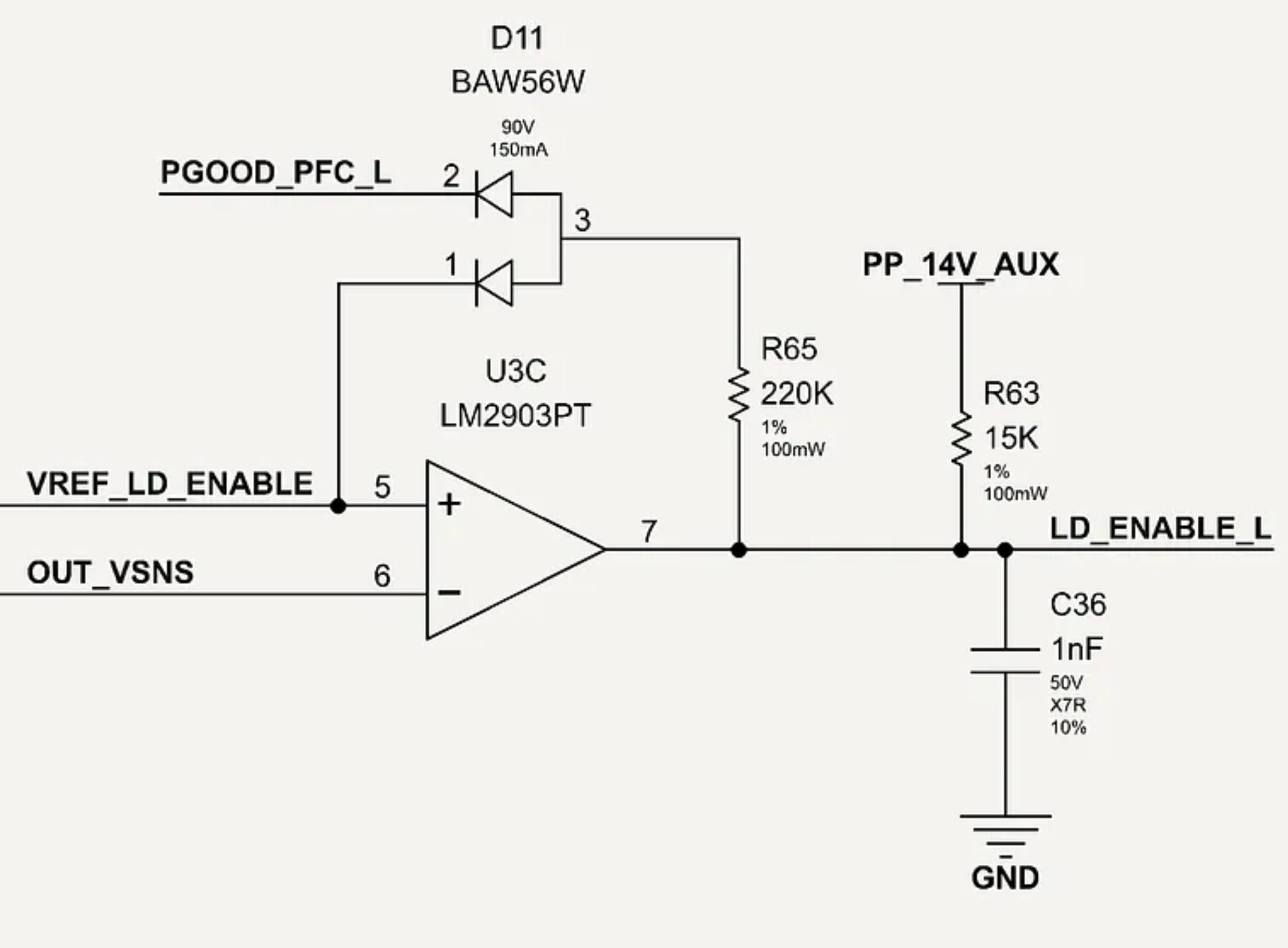
What this means is that once the boost converter has started up and LD_ENABLE_L has asserted, this circuit will latch. Even if the boost converter stops running due to a fault, the module will continue asserting LD_ENABLE. This is because even though PGOOD_PFC_L will deassert when the boost ceases functioning, it has no way to deassert LD_ENABLE_L, since the comparator is already grounding the line. This behaviour is also documented in the module’s datasheet:
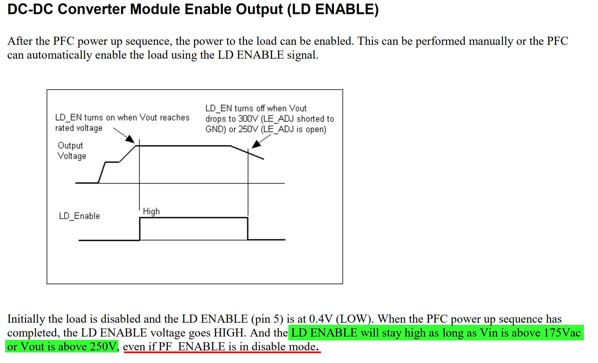
The only way to deassert LD_ENABLE is to either remove power from the system entirely, or deassert the PF_ENABLE pin. Contrary to the statement underlined in red above, this should work to force deassertion of LD_ENABLE.
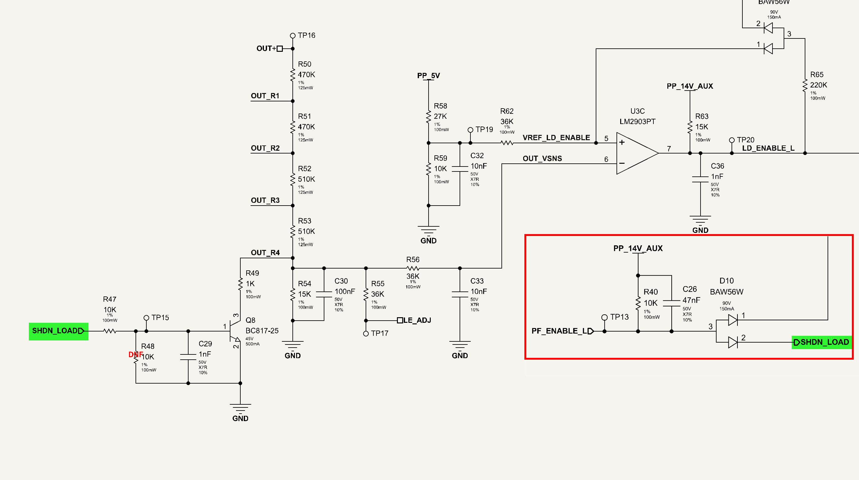
Releasing the PF_ENABLE pin will cause SHDN_LOAD to assert, which in turn will introduce a 1K resistor in parallel with R54 via Q8. This forces OUT_VSNS to a much lower voltage than 1.351V, which should force the comparator output to go hi-Z. Since PGOOD_PFC_L will also be already deasserted, LD_ENABLE will finally be able to deassert as well.
No posts
Comments
Nothing yet. Say the first thing.
Sign in to join the conversation.