
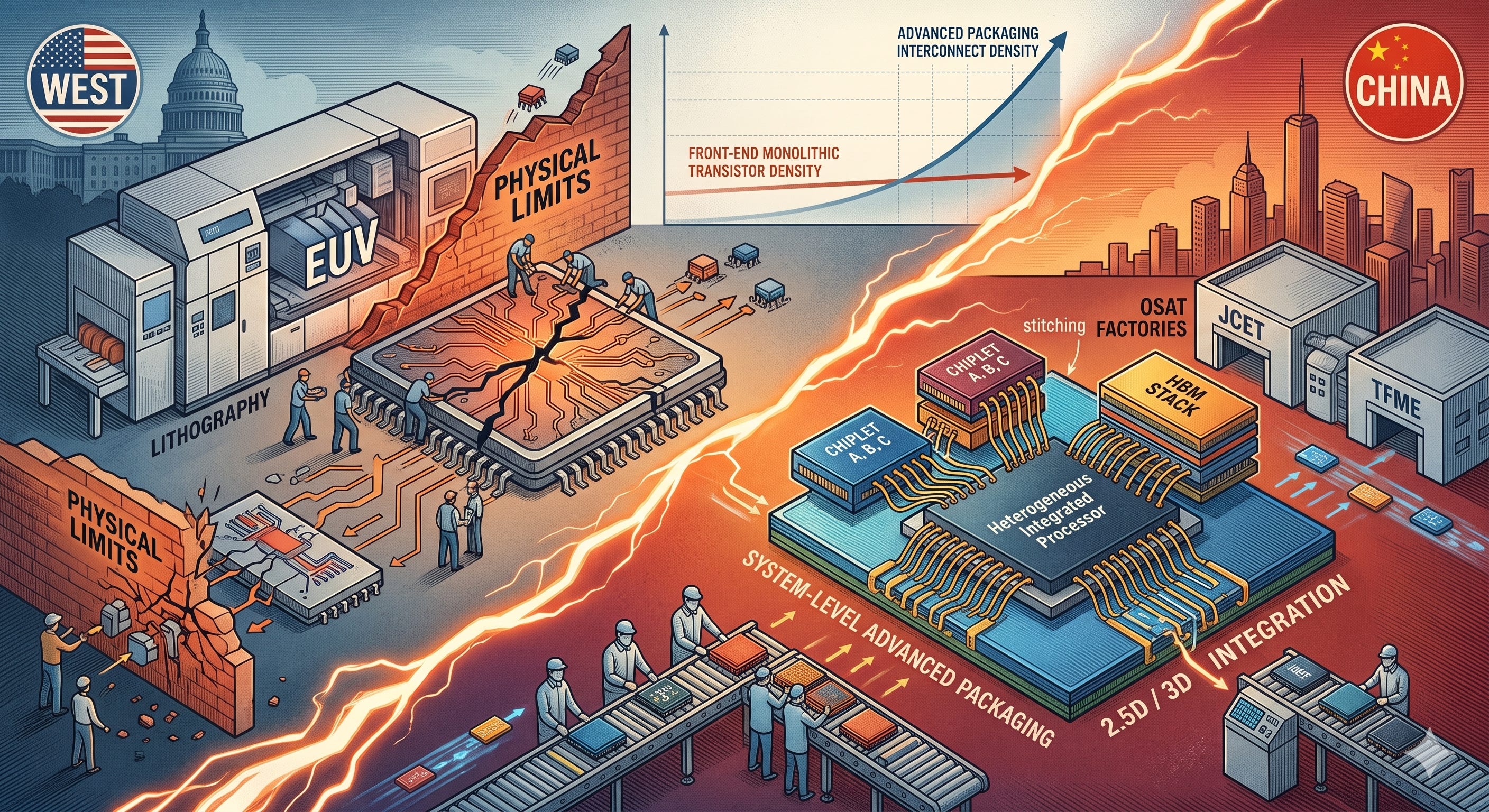
For over five decades, the semiconductor industry’s trajectory was dictated by Moore’s Law—a relentless march toward shrinking monolithic transistors. But as silicon nodes collide with harsh physical limits, the frontline of global chip supremacy has shifted from high-end lithography to advanced packaging. This is no longer a theoretical backend battle. As global AI infrastructure siphons away memory capacity—triggering a severe consumer DRAM crunch that has forced Apple to aggressively lobby Washington for access to Chinese memory giants like CXMT—advanced packaging and heterogeneous integration have emerged as the ultimate geopolitical chessboard. The winner of this war will not be the side that builds the smallest isolated transistor, but the side that controls the physical means to connect and scale them.
Industry veteran and former TSMC CTO Shang-yi Chiang frames this transition as a strategic pivot point: while front-end scaling once outpaced all other segments, it is now hitting hard physical limits. This has left advanced packaging as the primary frontier for silicon innovation.
Chiang maintains an “optimistic yet cautious” outlook, viewing advanced packaging as the next major domain for raw performance and speed gains. Historically dismissed as a low-margin, back-end logistical step, packaging has evolved into a strategic high-ground where the most significant system-level improvements are won.
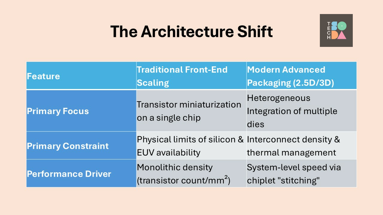
This technical transformation has ignited a global geopolitical race for “technology sovereignty.” Once packaging became the primary vehicle to extend system performance beyond the boundaries of optical lithography, it simultaneously became a potent strategic tool for nations looking to bypass traditional manufacturing bottlenecks.
Against this backdrop, Beijing’s semiconductor strategy is best understood not as a head-on attempt to replicate the West’s advanced lithography ecosystem, but as an asymmetric sidestep built entirely around packaging. To counter U.S. export controls on Extreme Ultraviolet (EUV) lithography, China has deployed an aggressive “Chiplet + Mature Node” strategy. This represents a fundamental shift toward a system-led design philosophy, extracting performance gains through high interconnect density and integrated High Bandwidth Memory (HBM) rather than raw transistor shrinking.
This “Lego-like” method involves splicing multiple mature 14nm or 28nm chiplets together to approximate the system-level performance of a 7nm or 5nm monolithic chip. Crucially, this approach relies on Lithography Compensation. Because domestic foundries rely on older Deep Ultraviolet (DUV) machines requiring complex multi-patterning, defect rates on massive monolithic chips are prohibitively high. By breaking designs into smaller, modular chiplets, manufacturers achieve far higher yields; defective individual dies can be discarded without scrapping the entire multi-chip processor, making DUV-based high-end computing economically viable.
Cost Efficiency: Operating at roughly one-fifth the cost of the traditional EUV-based monolithic route.
Compressed Delivery: Reducing cycle times by up to 60% by bypassing the severe global backlog for high-end lithography tools.
Yield Optimization: Utilizing smaller, discrete dies to inherently offset the technical inefficiencies of multi-patterning DUV.
The “Silent Revolution”: The 2026 debut of the Huawei Kirin 9030 Ultra chip demonstrated that performance rivaling traditional 7nm nodes is achievable without EUV hardware. By utilizing advanced 2.5D/3D packaging to stitch logic chips with domestic memory stacks, China has proven that high-end computing has alternative technological pathways. The remaining question is whether this strategy can scale beyond isolated breakthroughs into sustained industrial infrastructure.
This asymmetric strategy has crystallized into a formal, industry-altering semiconductor design framework. At the 2026 IEEE ISCAS conference, Huawei’s semiconductor head He Tingbo officially introduced the Tau (τ) Scaling Law. This law proposes a fundamental paradigm shift: replacing traditional geometric scaling (shrinking transistors) with temporal (τ) scaling (compressing the time delay of data traveling across a system).
Central to the Tau Law is Huawei’s “LogicFolding” architecture. Rather than laying out circuits across a flat, 2D plane, LogicFolding vertically layers and “folds” circuits in a 3D layout to radically shorten critical path wiring and eliminate latency bottlenecks.
[Traditional Geometrical Scaling]      [Huawei Tau (τ) Temporal Scaling]
     Shrink Transistors (2D)                 Fold Circuits Vertically (3D)
  ┌───┐ ┌───┐ ┌───┐                       ┌───┐
  │   │ │   │ │   │  ──► Node Limit       ├───┤ ◄── Shortened Path (LogicFolding)
  └───┘ └───┘ └───┘                       └───┘
Crucially, this architectural leap is entirely impossible without advanced packaging. To achieve a projected density equivalence of 1.4nm (14 Å) by 2031 without bleeding-edge EUV lithography, Huawei is dependent on high-density 2.5D/3D integration, ultra-fast silicon interposers, and advanced wafer stacking. The Tau Law signals that China is no longer merely attempting to catch up to the West’s lithography roadmap; it is actively weaponizing advanced packaging to redefine the metrics of chip performance entirely.
China’s competitive edge is anchored by a massive industrial base, currently housing approximately 30% of global packaging infrastructure across more than 92 facilities. This dominance is reinforced by a stark economic reality: building and operating cleanrooms in the U.S. costs roughly 50% more than in Taiwan or mainland China.
China’s packaging push is not merely a technology workaround; it is a massive scale and cost play. This cost divide is so pronounced that even U.S. giants like Intel continue to expand their packaging footprints in China despite receiving multi-billion-dollar domestic subsidies in the West.
This ecosystem is the product of a decades-long seeding of human capital. Before 2010, Taiwanese packaging leader ASE trained over 500 mainland Chinese engineers to strengthen its supply chain in Taiwan and China. However, due to deteriorating cross-strait relations and China’s policy to foster its domestic OSAT industry, those ASE-trained engineers eventually dispersed across China’s 200+ domestic Outsourced Semiconductor Assembly and Test (OSAT) firms, with many now serving as top executives and lead architects. Today, this growth is sustained by three state-backed mechanisms:
Mega-Subsidies (The “Big Fund”): Multi-billion dollar capital pools providing low-interest loans for aggressive, continuous capacity expansion.
Localization Mandates: Strict domestic requirements for tech firms to prioritize local packaging suppliers, driving revenue growth three to eight times faster than the global average.
R&D Strategic Financing: Direct capital injection targeting the transition from traditional wire-bonding to high-density 3D integration and silicon interposers.
Chinese players are aggressively climbing the global Top 10 rankings, characterized by double-digit revenue growth and significant net profit surges.
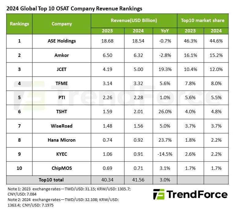
A deep dive into the data from Trendforce’s 2024 Top 10 OSAT Ranking Report (this is the latest report currently available) reveals a stark divergence in performance between established Western/Taiwanese leaders and rising Chinese OSATs, underscoring the structural shift underway:
The Growth Divergence (The Aggressive Catch-Up): While the global Top 10 OSAT revenue grew at a modest aggregate rate of 3.0% from 2023 to 2024, China’s core players dramatically outpaced the market. TSHT (HT-Tech) exploded by 26.0% YoY, and JCET surged by 19.3% YoY. Conversely, market leaders ASE Holdings (-0.7%) and Amkor (-2.8%) saw negative growth, indicating that market expansion is being heavily captured by mainland Chinese firms capitalizing on localized chiplet and mature-node demand.
Encroaching Market Share: The market share concentration is shifting at the top. Traditional heavyweights ASE and Amkor collectively shed 2.6% of the Top 10 market share in 2024. This exact chunk was entirely eaten up by mainland Chinese players: JCET grew its market share from 10.4% to 12.0%, and TSHT climbed from 4.0% to 4.8%.
Dominance in Numbers: Of the global Top 10 listed in Trendforce’s 2024 ranking, four entities—JCET (#3), TFME (#4), TSHT (#6), and WiseRoad (#7)—are mainland Chinese firms. When adding specialized pure-plays like SJ Semiconductor (which operates heavily in high-value 2.5D integration and anchors the tail-end of top rankings), China commands nearly half of the world’s leading OSAT slots by company count.
The data proves that China’s “asymmetric packaging strategy” is no longer a theoretical threat; it is reflected directly in corporate revenue. The massive capital injections from Beijing’s “Big Fund” and localization mandates are allowing Chinese OSATs to maintain double-digit growth velocity even during macroeconomic downturns that caused negative growth for standard global market leaders.
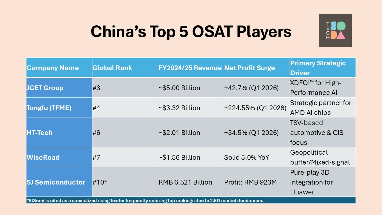
The technical sophistication of China’s “Big Three” and rising specialized players now rivals global leaders in specific high-density architectures:
JCET Group: Leads with proprietary XDFOI™ technology, enabling ultra-high-density 2.5D/3D multi-chip integration targeted at AI workloads.
Tongfu (TFME): Serves as the primary backend partner for AMD, specializing in complex, multi-chip module server architectures.
TSHT-Tech: Focuses on Through-Silicon Via (TSV) and wafer-level packaging optimized for high-reliability automotive sensors and high-performance computing (HPC).
SJ Semiconductor (SJSemi): A pure-play 3D integration leader unburdened by legacy overhead; it commands an estimated 85% share of China’s domestic 2.5D packaging market.
[x] 2.5D Silicon Interposers: (JCET, SJSemi, HT-Tech)
[x] 3D Multi-Chip Heterogeneous Integration: (SJSemi, TFME, JCET)
[x] Fan-Out Wafer Level Packaging (FOWLP): (JCET, HT-Tech, TFME)
[x] Wafer Bumping (12-inch Mid-End): (SJSemi, JCET)
Despite this momentum, three critical bottlenecks threaten China’s domestic industry’s path toward absolute self-sufficiency:
Comments
Nothing yet. Say the first thing.
Sign in to join the conversation.