
The Dutch Circle of Slide Rule Collectors hosts regular International Workshops open to all slide rule collectors to discuss ‘mystery’ slide rules submitted by slide rule collectors globally. The 5th such two-hour workshop was held last month on Sunday June 14, 2026.1
One of the submissions for discussion at the workshop was a special-purpose slide rule manufactured by Nestler, with the company name ‘Wacker’ on the rule. The rule was submitted by Nestler expert Andreas Faßbender.2 Some preliminary investigations into the rule by Andreas revealed that it was targeted towards silicon integrated circuit manufacturing. It incorporates several scales for computing the size and weight of silicon wafers, and the resistivity of P-type and N-type silicon semiconductors.
I have several slide chart calculators with scales that perform essentially the same calculations, including a few that were also made for Wacker. In this article we’ll take a look at the computations made possible with the slide charts and Nestler slide rule.
Integrated circuits (ICs) refer to complete electronic circuits that are manufactured on a single piece of semiconducting material. The most commonly used semiconductor is silicon, but germanium and gallium arsenide are also used.
ICs are made from highly purified crystals of silicon in the shape of a cylindrical bar. These are formed by first melting highly purified quartz sand in a quartz crucible at 1410°C, then dipping a crystal “seed” into the hot liquid and slowly pulling it up while spinning. As the silicon cools, it forms a large mono-crystal in the shape of a cylindrical bar.
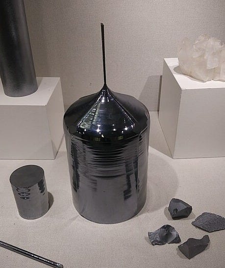
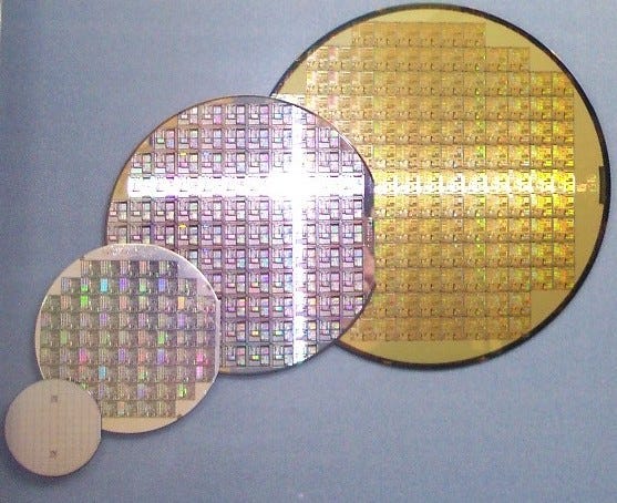
The silicon bar is then sliced into thin disks and the circuits are etched onto these disks using photo-lithography processes. Multiple copies of the same IC are etched onto the wafer during the IC manufacturing process. The wafer is then sawn into individual ‘dies’ which are packaged and sold as the integrated circuits.
Pure crystal silicon is neither a good insulator nor a good conductor of electricity (hence the term semiconductor). Its conductivity can be changed by mixing in a few atoms of other materials. This process is called doping.
Silicon has four electrons in its outer band. When silicon is doped with atoms that have five electrons in their outer bands, e.g., phosphorus or arsenic, four of the electrons from each dopant atom bond with the neighboring silicon atoms in the crystal lattice. The extra electrons are free to roam and conduct electricity. Since it has a negative charge, the result is called an N-type semiconductors.
Conversely, when silicon is doped with atoms that have three electrons in the outer bands, e.g., boron or gallium, a hole is created when the dopant atoms bond with the neighboring silicon atoms in the crystal lattice. Electrical conductivity is improved because neighboring electrons can jump from hole to hole. The result is called a P-type semiconductor.
When a piece of P-type semiconductor is adjacent to a piece of N-type semiconductor, they form a P-N junction, which is the basis for many electronic components including diodes and transistors. The electrical properties of these components depend on the amount of atoms of other materials that are used to dope the silicon crystal.
The earliest semiconducting devices based on P-N junctions were diodes (invented in the 1940s) which conduct electricity flowing in one direction and block it in the other, and transistors (invented in 1947) which can amplify electrical signals. By the mid-1950s individually packaged transistors and diodes made from silicon and germanium were widely available, but wires or conductive traces on printed circuit boards were still required to connect the components in a circuit together.
In September 1958 the first IC made from germanium was demonstrated by Jack Kilby at Texas Instruments. All components in the circuit were integrated on the same piece of material, although gold wires were still used to interconnect the components.
In 1959, the first silicon IC was built by Robert Noyce at Fairchild Semiconductor. In this IC, the components and the interconnect between components were all built on the same piece of silicon. By 1961 Fairchild was producing and selling commercial ICs. One of the biggest early customers for ICs was NASA, where the Apollo program was the largest consumer of integrated circuits from 1961 - 1965.
The first slide chart with scales for computations related to designing and manufacturing ICs was the Dow Corning Silicon Slide Rule, made by Perrygraf in 1962. Dow Corning was manufacturing pure bars of silicon for the semiconductor industry since 1959 from their factory in Hemlock, Michigan.
This rectangular slide chart has scales for computing the size, area and weight of silicon wafers, the weight of silicon bars, and for determining the resistivity of N-type and P-type silicon semiconductors, give the dopant concentration in parts per billion atoms, or atoms per cubic centimeter. A table of silicon properties is also provided, along with references for the data appearing on the slide chart.
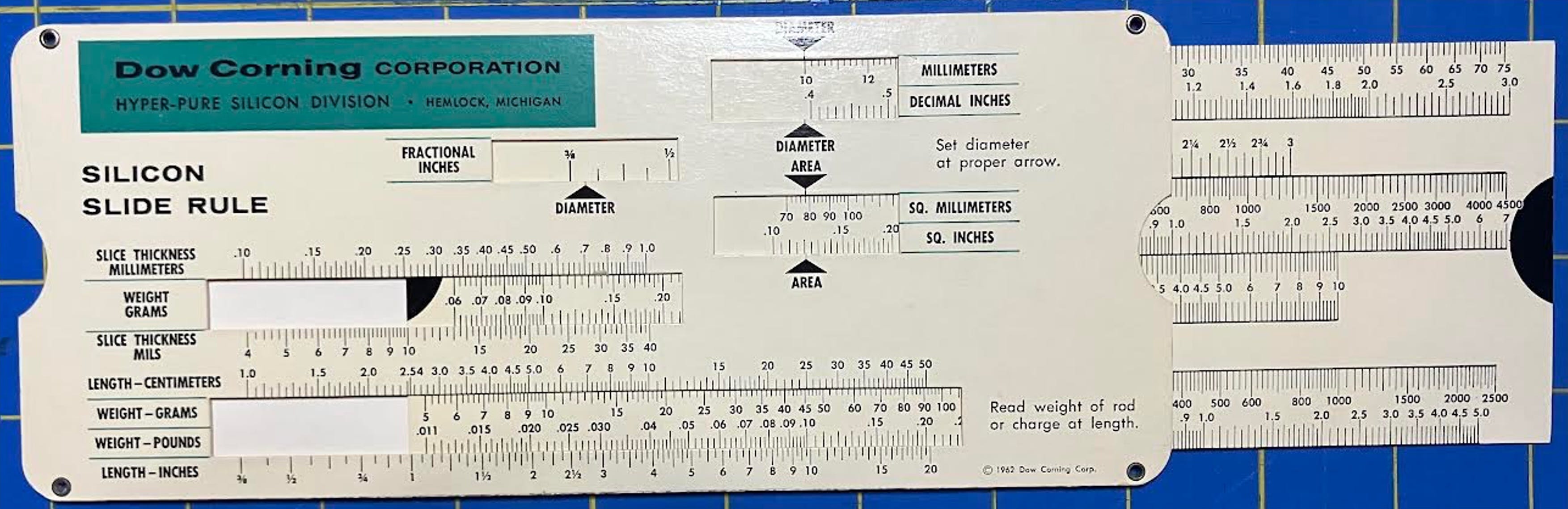
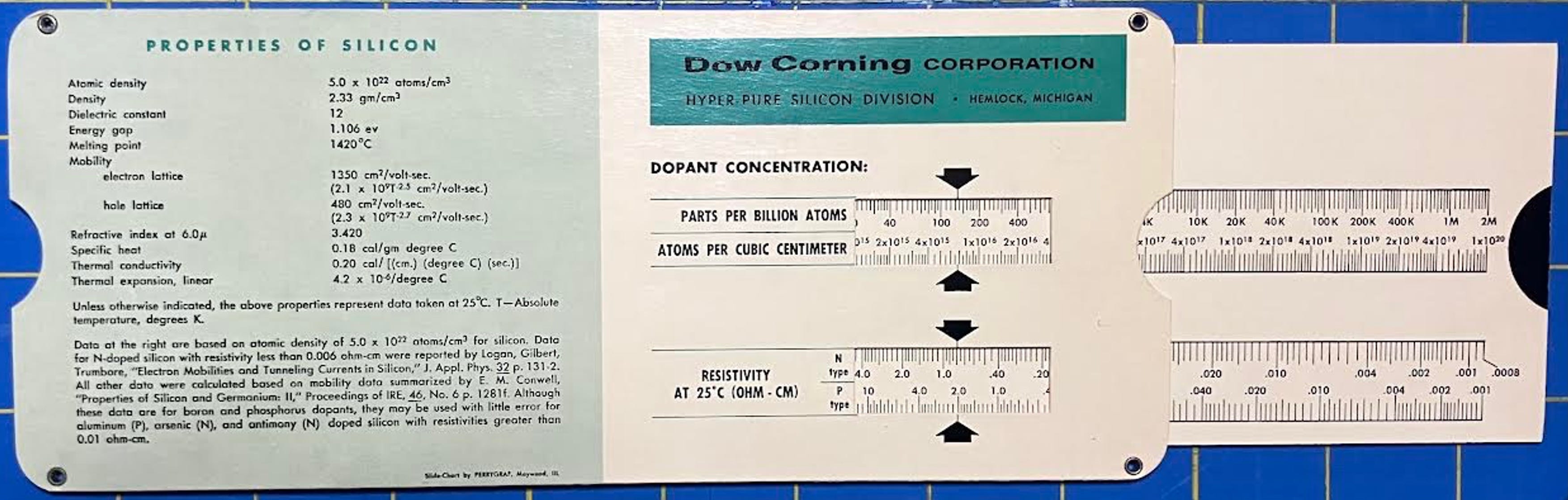
The following calculations can be performed using the Silicon Slide Rule. Future versions of the slide chart also supported these calculations:
Silicon wafer area and diameter
Five scales on the upper front of the slide chart allow the area of a wafer to be computed when given the diameter, in metric and imperial units.
Silicon wafer size and weight
Three scales in the middle front of the slide chart are used to compute the weight of silicon wafer disk, given the diameter and thickness of disk. The weight is given in grams on all the slide charts.
Silicon bar size and weight
Four scales at the bottom front of the slide chart are used to compute the weight of a silicon bar, given the diameter and length of the bar. On this slide chart the weight is given in grams and in pounds. Future slide charts only give the weight in grams.
Resistivity of silicon in ohms-cm
The back of the slide chart has scales that give the resistivity for N-Type and P-Type silicon, given the dopant concentration in parts/billion atoms, or atoms/cc of silicon.
The scales on the slide chart are very well labeled. Basic usage instructions are provided on the face of the chart, making it straightforward and easy to use. The ranges of values on several of the scales are of note:
Values on the diameter scale range from 10 mm to 75 mm (0.4 inches to 3.0 inches). In 1962 pure silicon bars were typically 1 inch in diameter. Clearly the chart designer was anticipating that the diameter of silicon bars would increase over time.3 The diameter scale range was also increased on later iterations of the silicon slide rule, as the diameter of silicon bars continued to grow. Nowadays, silicon bars of 12 inches in diameter are used for high volume state of the art ICs, and researchers are working on introducing 18 inch diameter bars for future wafer fabrication facilities.
The atoms per cubic centimeter scale has values ranging from 6×10¹¹ to 1×10²⁰. It’s very unusual to see values of this magnitude on a slide rule or slide chart scale.
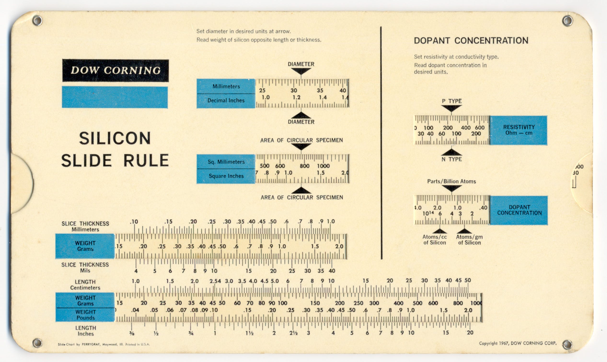
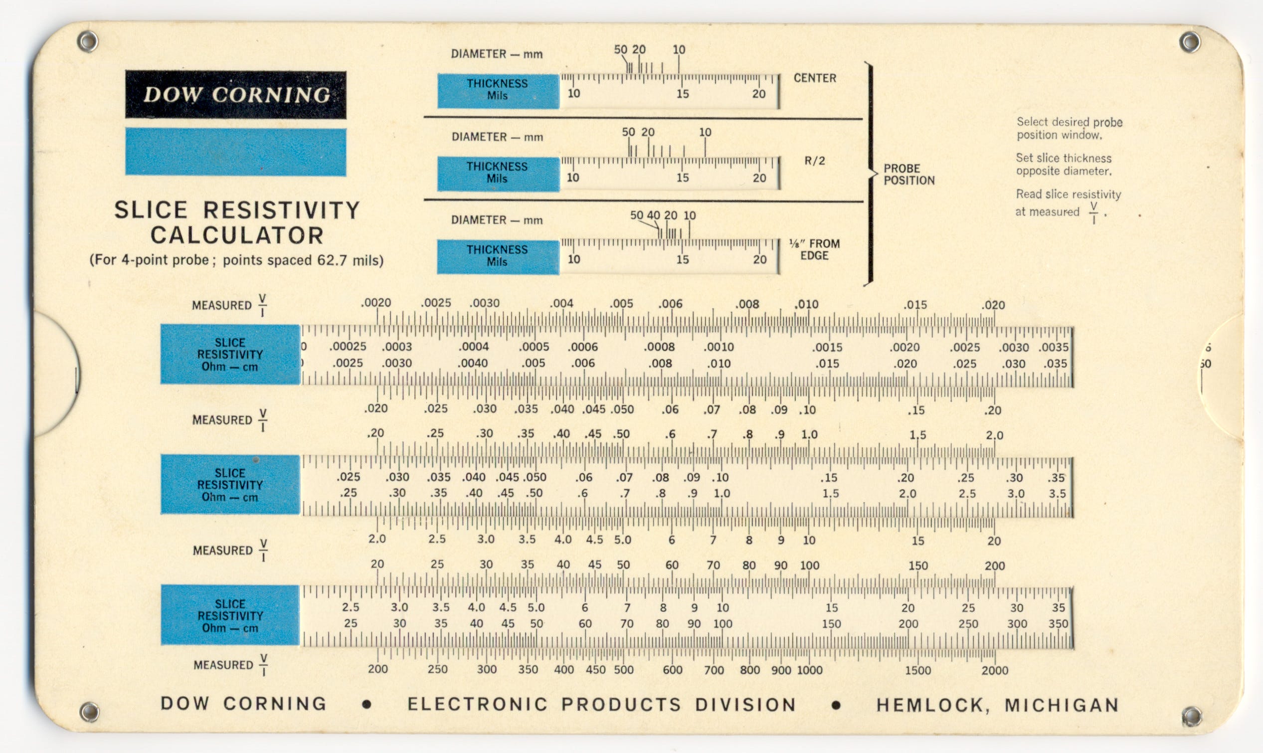
An updated version of the 1962 Dow Corning Silicon Slide rule was made by Perrygraf in 1967. It performs all the calculations of the 1962 slide chart, but the scales for these calculations are all moved to the front side of the chart. The wafer diameter scale range has increased from 3 inches on the 1962 chart to 6 inches on this chart, and the ranges on other scales have correspondingly increased. The back side of the chart is now labeled Slice Resistivity Calculator. An entirely new set of scales has been added to compute the resistivity of silicon slices in ohms-cm based on the voltage and current measured by a test probe with points spaced 62.7 mils (0.0627 inches) apart. The table of silicon properties has been removed to make room for the new scales.
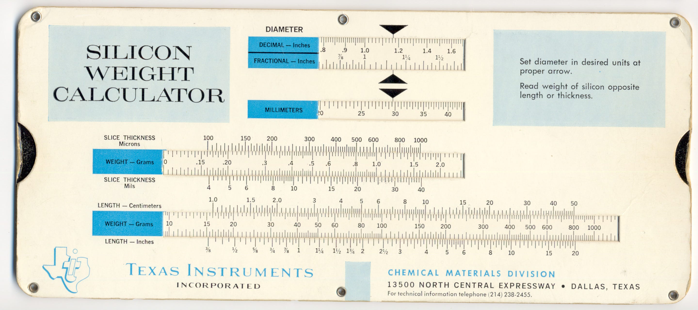
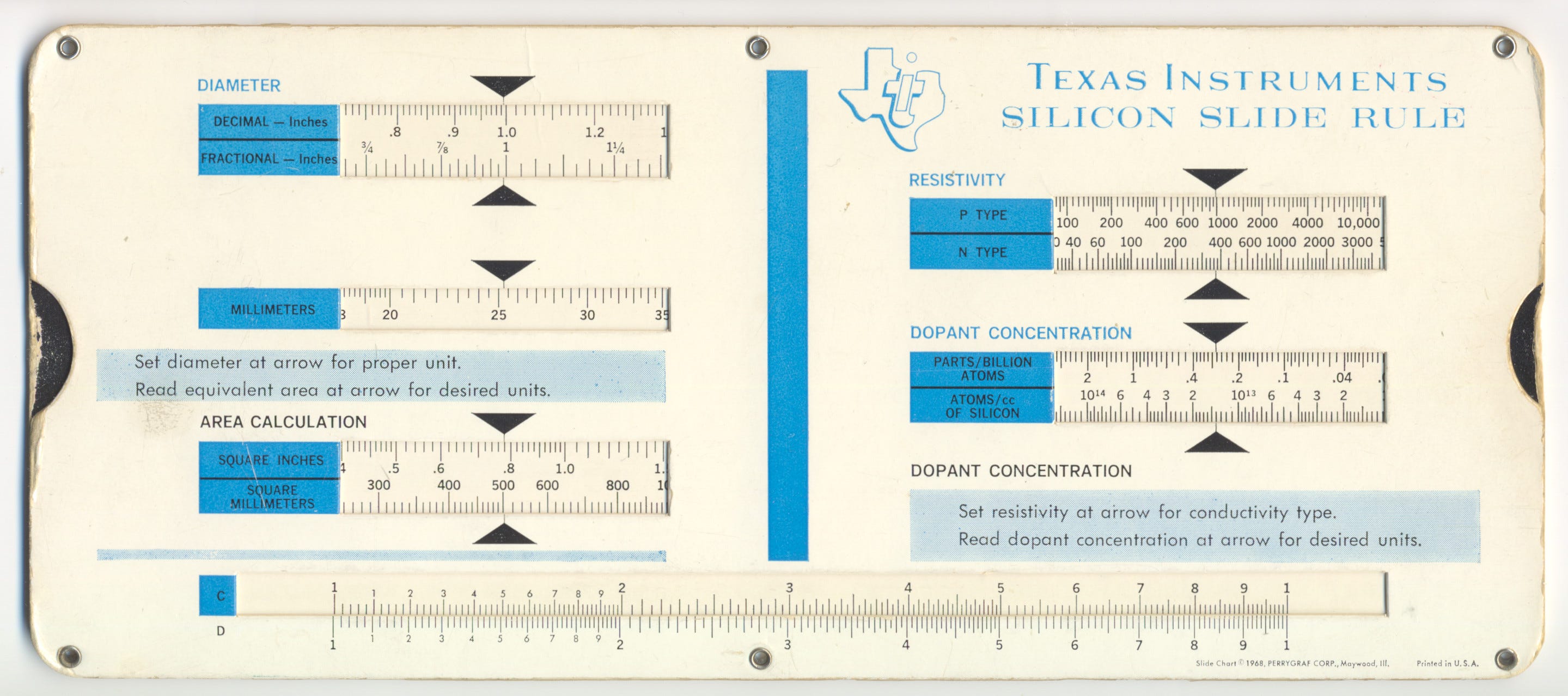
In 1968, Perrygraf made a variant of the 1962 Dow Corning Silicon Slide Rule for Texas Instruments. This has essentially the same scales as the 1962 Dow Corning chart, but they have been rearranged, with the silicon weight scales kept on the front, and the silicon wafer dimension and resistivity scales moved to the back. The weight scale in pounds has been removed, and the slice thickness is given in microns, instead of in mm. The wafer size and weight scale ranges have also increased to allow calculations with wafers up to 5 inches in diameter. Standard slide rule C and D scales are also added on the back allowing general purpose calculations to be done while the chart is in-hand. There is no table of silicon properties on the chart.
In 1968 Nestler manufactured a slide rule for Wacker Chemie, a German multinational chemical company, with scales capable of doing essentially the same calculations as the earlier Perrygraf slide charts. Wacker was founded in 1914 and had been in the semiconductor business since 1953, producing silicon wafers by 1962. The Wacker Chemitronic subsidiary was founded in 1968 to focus on the production of hyper-pure silicon for the electronics industry. It’s likely that the slide rule was commissioned as a result of the founding of the Wacker Chemitronic subsidiary.
The Nestler Wacker slide rule is very high quality, being built on the same frame as high-end Nestler slide rules of the era, such as the Nestler 0291 Polymath Duplex, Nestler 0292 Multimath Duplex and Nestler 0297 Electronics slide rules. This is a much more robust and longer-lasting device than the slide charts discussed in this article. Unfortunately, at this time there is no known manual for the slide rule. Andreas researched the scales on the slide rule and his findings are documented here.
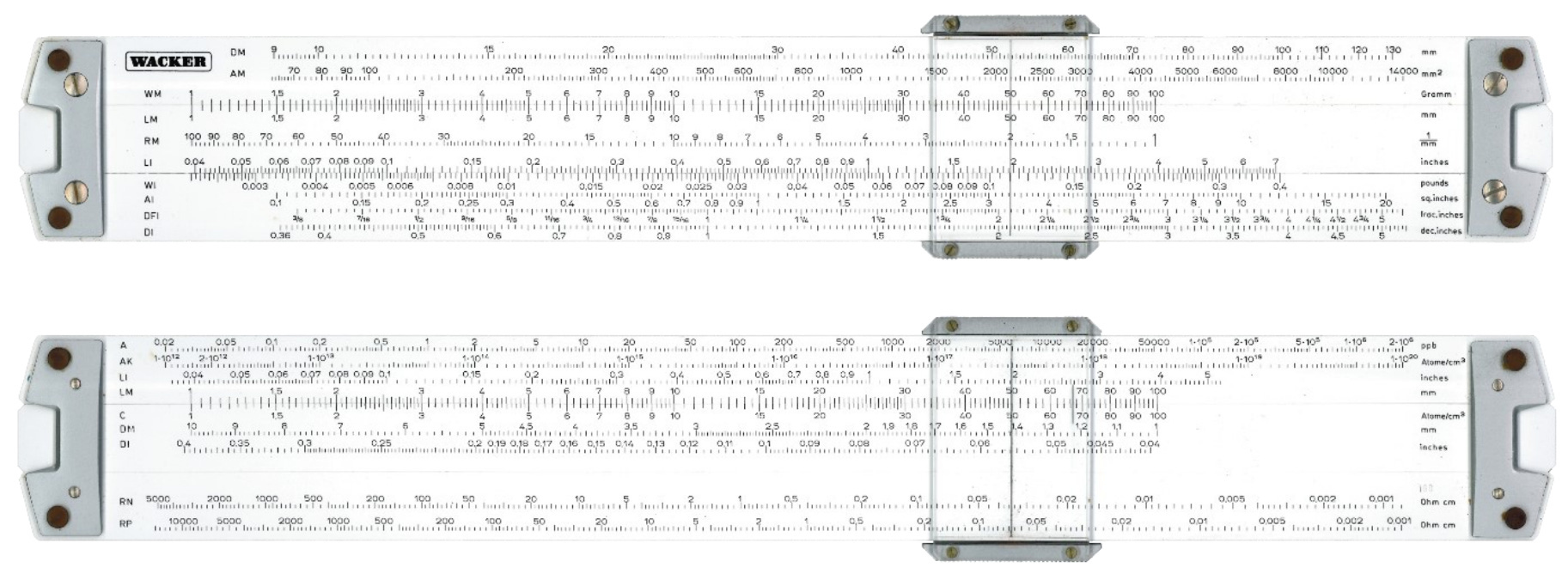
The 10 scales on the front of the Nestler Wacker rule and 4 of the scales on the back of the rule (A, AK, RN and RP) are used to perform the same computations as on the Perrygraf slide charts. The rule is not as intuitive to use as the slide charts we looked at earlier. Using the Perrygraf charts as a reference, I determined slide and cursor movements for carrying out the same computations that we looked at earlier - these steps are shown in Appendix A.
The Nestler Wacker rule also has 5 scales on the reverse side (LI, DI, LM, DM, C) for a calculation that is not yet known. The scale ranges don’t match those of any of the scales on the slide charts. The atoms/cm3 scale values range from 1 to 100, which is very low compared to the other atoms/cm scale where the range of values is from 1012 to 1020.
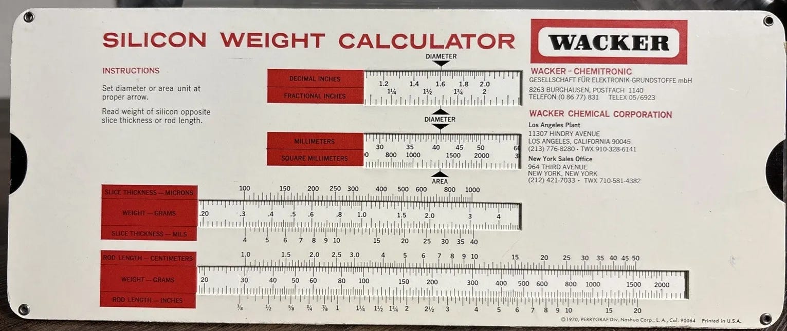
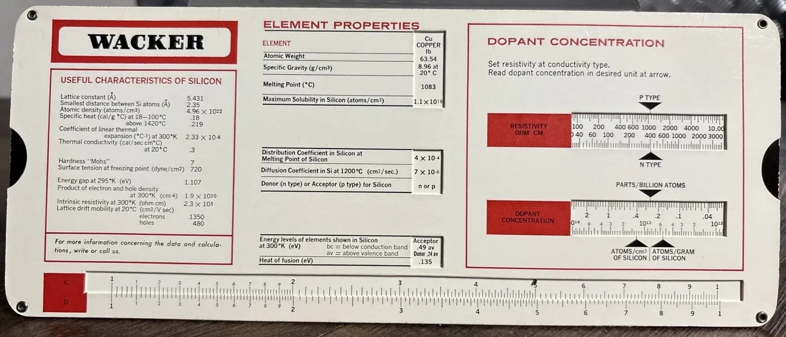
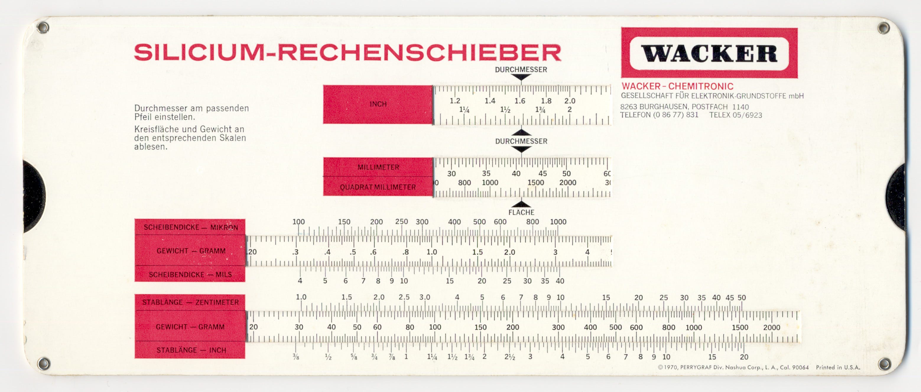
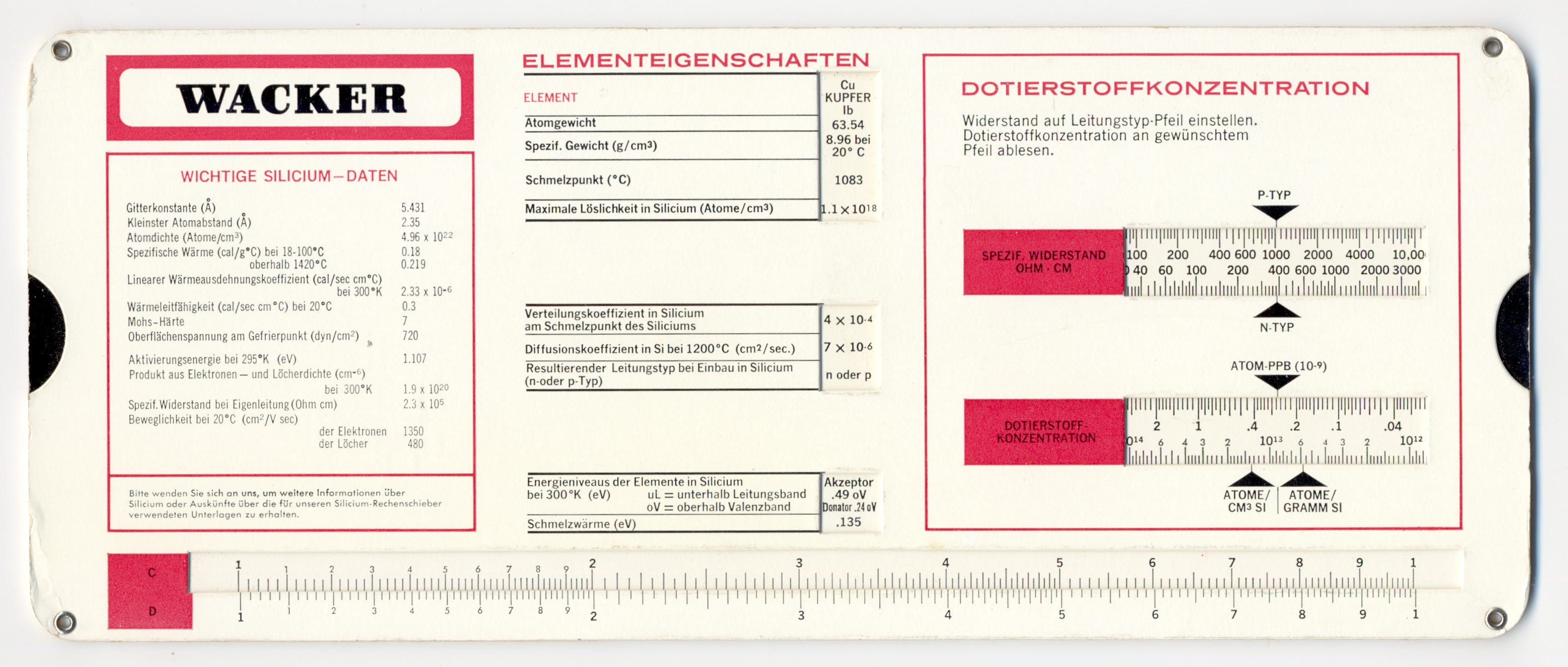
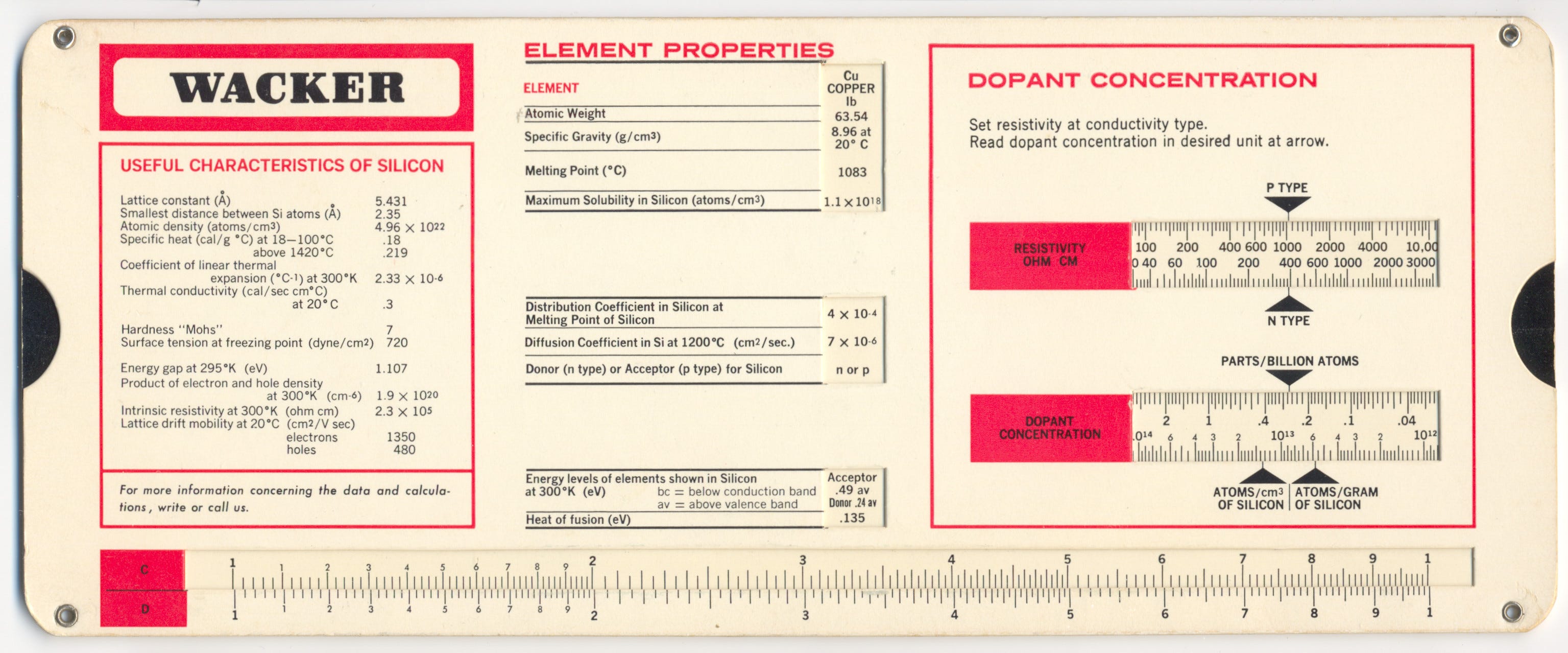
This is a variant of the earlier Perrygraf-made slide charts, made for Wacker Chemitronic. It has the same scales as the 1967 TI Silicon Weight Calculator, but with slightly different ranges. It also has a table of useful silicon data, as well as a sliding lookup table of element properties for 23 elements. Two versions of the slide chart were made, one in English, and an equivalent version in German. The English language version has the address of Wacker’s German and US offices, while the German language version only has the german office address listed.
English-language version:
German-language version:
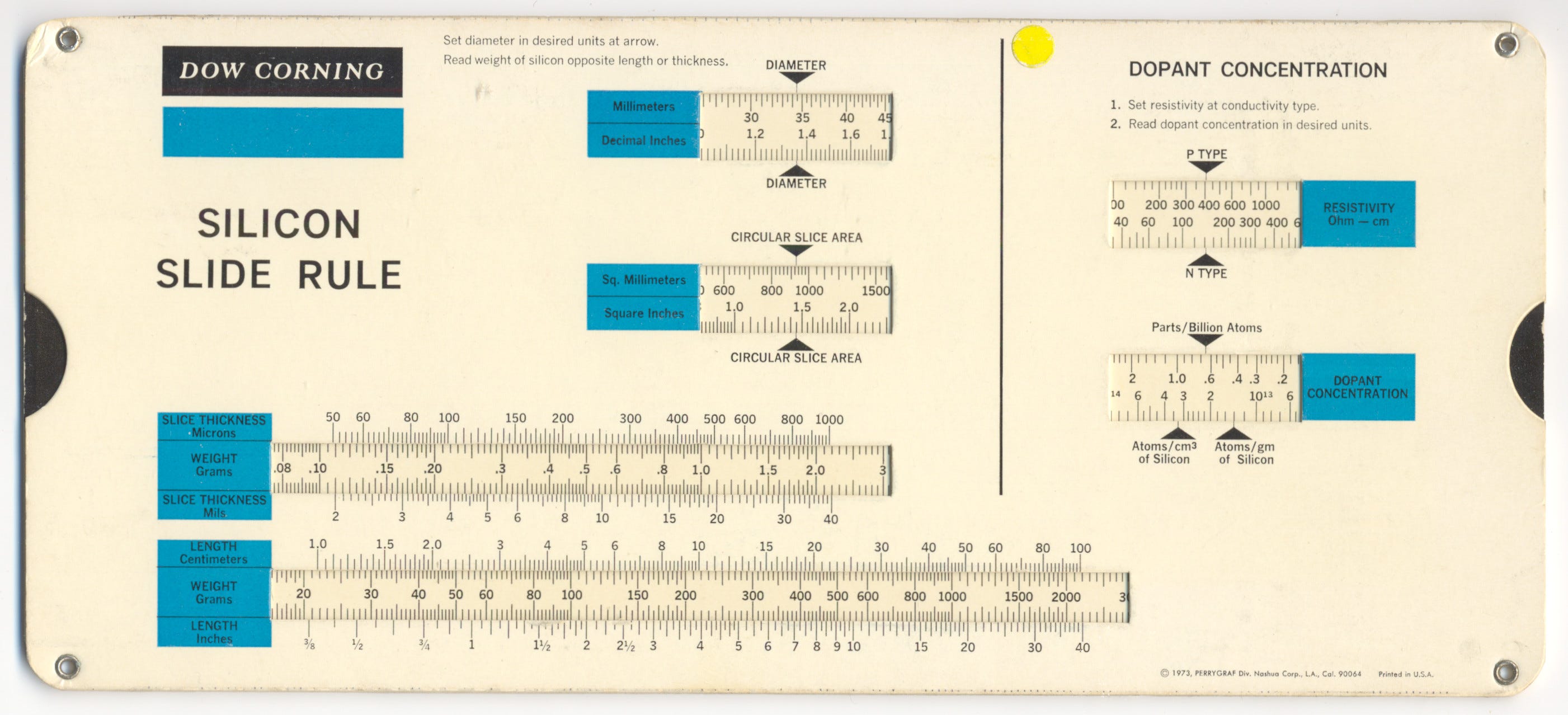
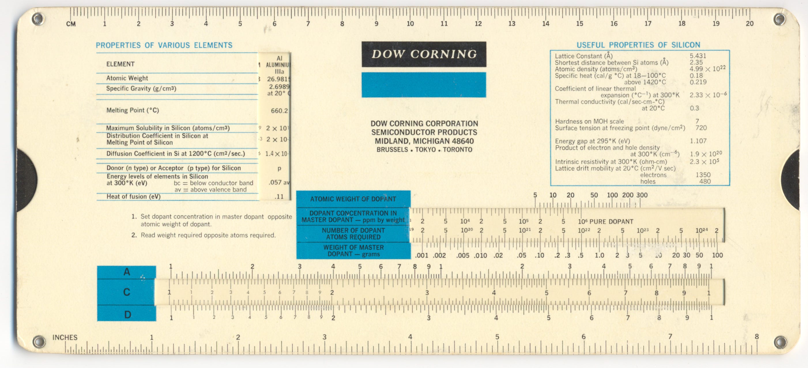
In 1973, the Dow Corning Silicon Slide Rule was updated again. The slide resistivity scales are no longer included. Instead, the rule has additional scales for Dopant Concentration calculations, that don’t appear on the other rules shown. This includes a scale for the number of Dopant atoms required, which has values ranging from 1×10¹⁵ to 1×1025. The table of silicon properties that appears on the Wacker slide chart is also included on this chart.
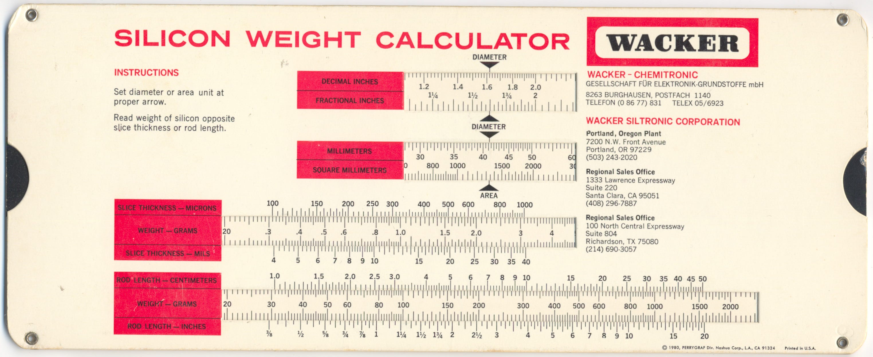
This is a straightforward re-issue of the Wacker Silicon Weight Calculator from 1970. The scales and scale ranges are indeed the same on each version. A new addition is the address for Wacker Siltronic Corporation in Portland, Oregon. This Wacker subsidiary was formed in 1978, just a couple of years before the calculator was made. We have not yet encountered a German-language version of the 1980 Wacker chart.
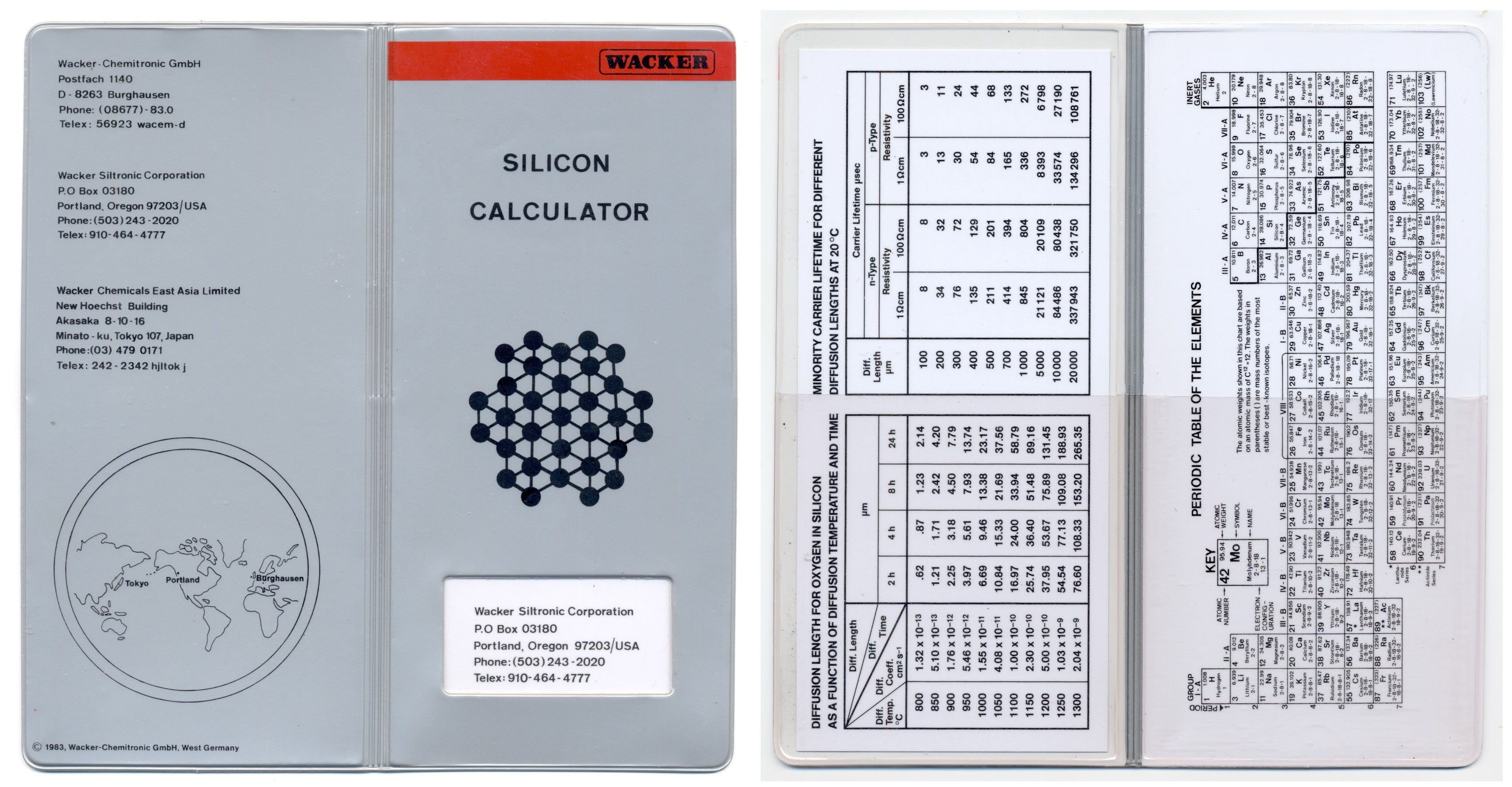
This is the last known version of the silicon slide charts. Unlike earlier versions, this one is made of plastic. It comes in a nice high quality protective plastic sleeve with a table of the elements on the inside. The chart retains the scales found on the earlier slide charts and adds a scale for computing electron and hole carrier mobility, given the dopant concentration.
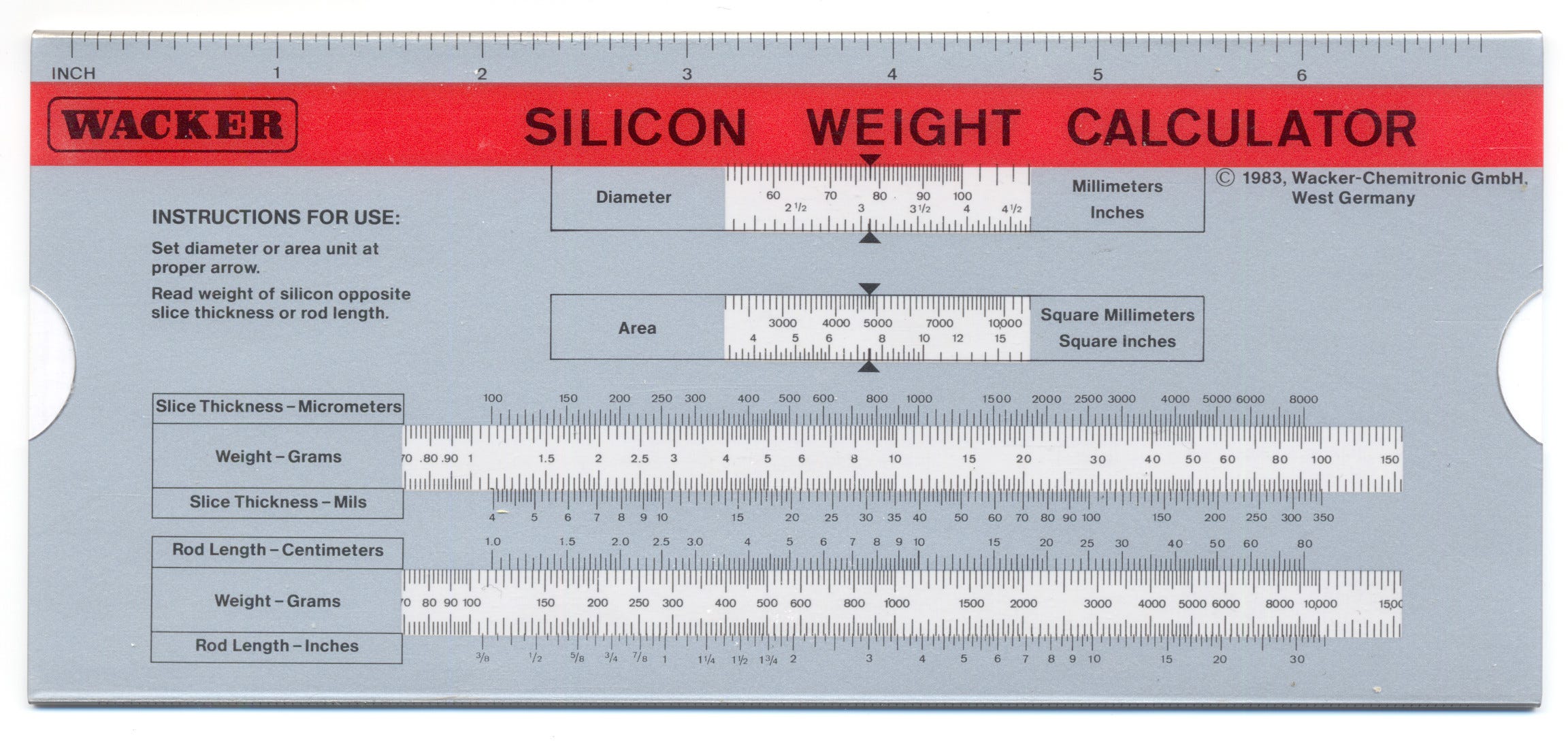
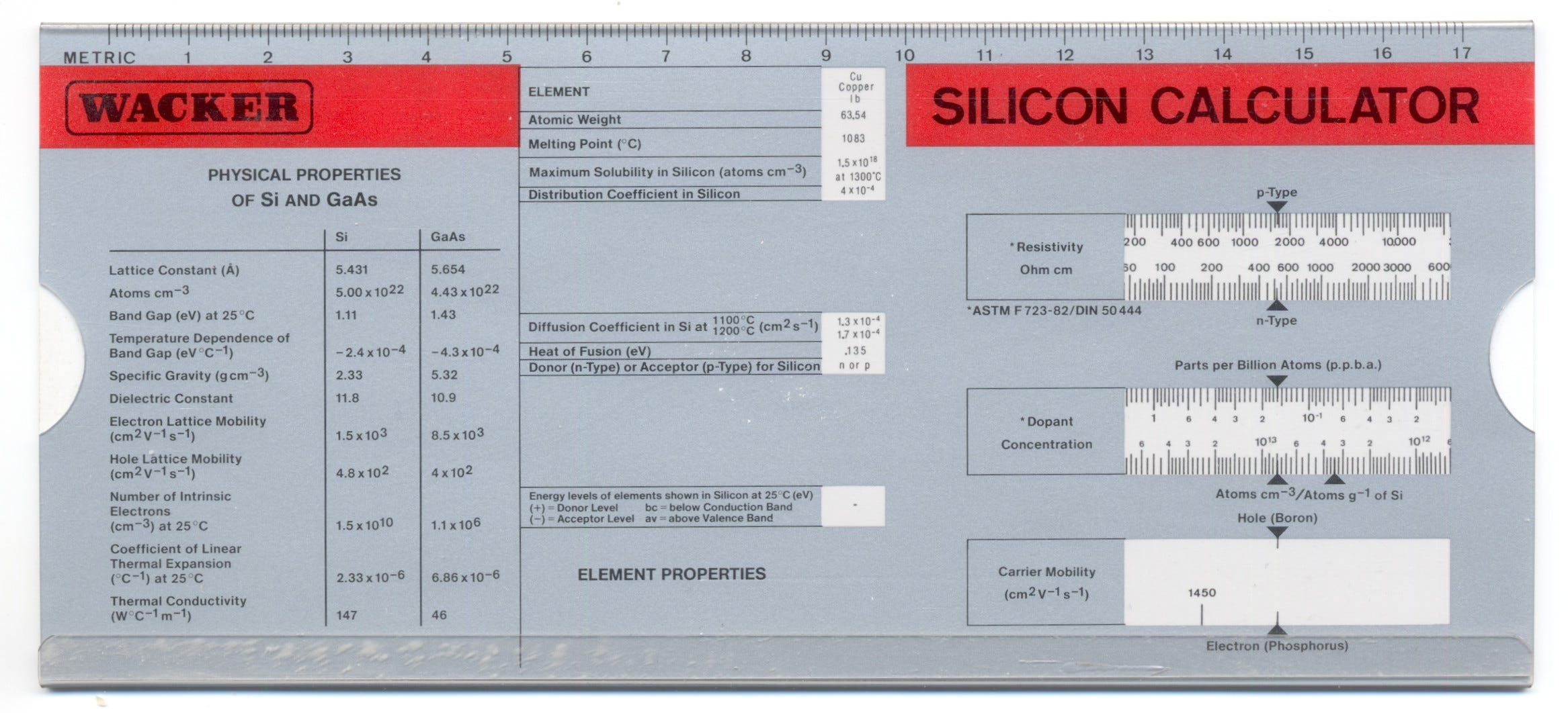
The following table shows the ranges of values of the scales on each of the slide charts and slide rule described in this article. The evolution of scale ranges common to each rule, reflecting the state of silicon manufacturing technology at the times the charts were made, and the scales unique to each iteration of the chart can be seen in the side-by-side comparison
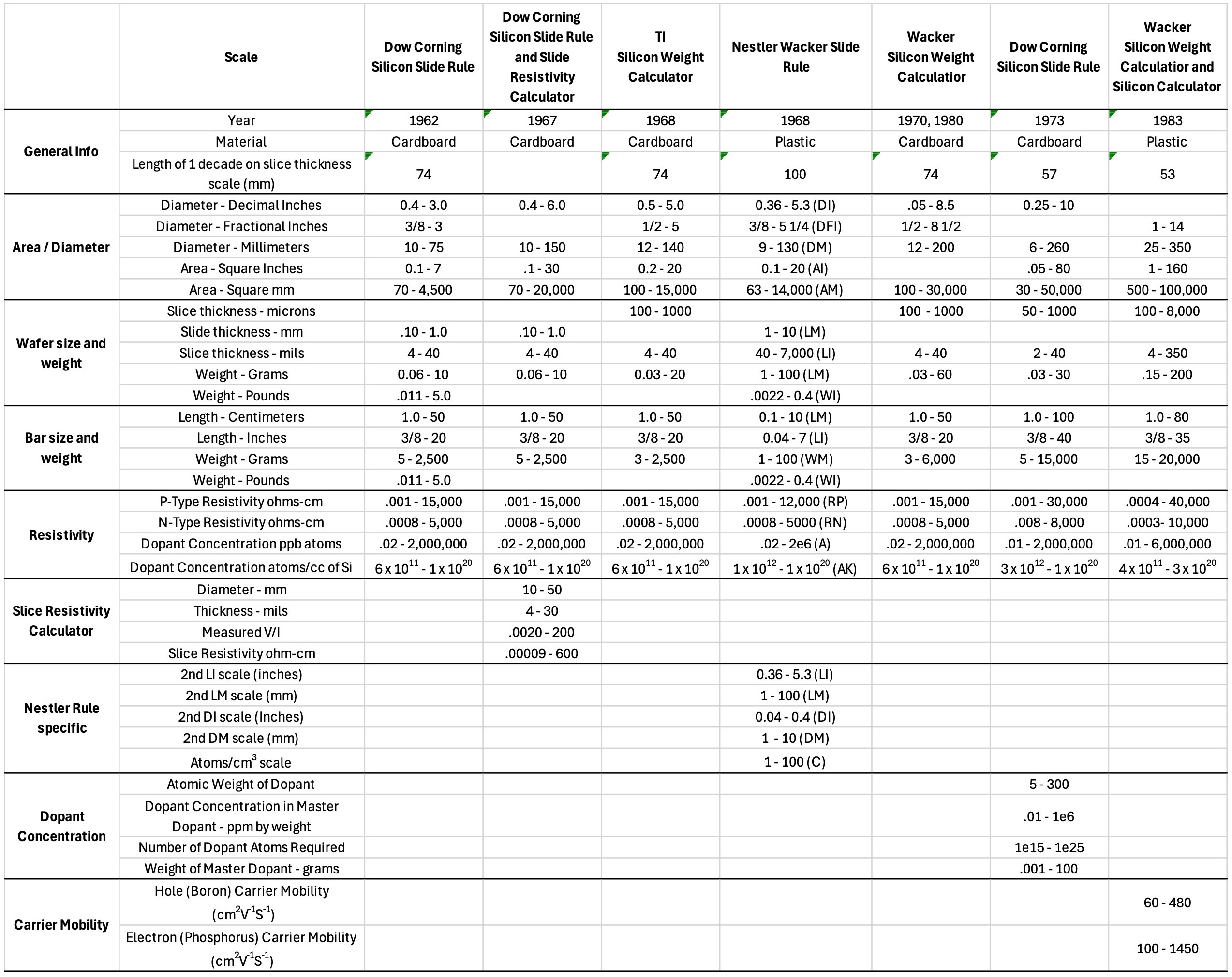
The maximum silicon bar diameter supported on the 1962 Dow Corning Slide chart is 3.0 inches. This increased to 6.0 inches on the 1967 Dow Corning chart, dropped a little to 5.0 inches on 1968 TI chart, increased again to 8.5 inches on the 1970 Wacker slide chart, to 10 inches on the 1973 Dow Corning slide chart and to 14 inches on the 1983 Wacker calculator.
The maximum bar length supported by the slide charts stayed at 50 cm until 1973, when it increased to 100 cm. The max weight supported on the charts increased over time to accommodate the increases in max wafer diameter, and max bar length.
The resistivity scale ranges are essentially the same from chart to chart.
The ranges of the diameter, area, and slice thickness/length scales on the Nestler Wacker rule are smaller than on the slide charts. For example, the bar length scale only extends to 10 cm, while on the slide charts it extends to either 50 cm or 100 cm. This means that the length of one decade on these scales is longer than one decade of these scales on the the slide charts. Computations done on the Nestler rule will therefore be more accurate than on the slide charts. However, the reduced ranges of the diameter, area and weight scales on the Nestler means that the user needs to pay close attention to determine the position of decimal point in the final result. This is generally not an issue with the slide charts.
The logical grouping of the scales and the labeling of the scales on the slide charts makes them straightforward to use. The scales on the slide rule are less intuitive to understand, mainly due to the more terse scale labeling required for the slide rule.
We have seen several silicon slide charts made by Perrygraf and one silicon slide rule made by Nestler, with scales for computations related to manufacturing silicon wafers and integrated circuits. It’s notable that the first of these slide charts appeared in 1962, shortly after the development of the first experimental integrated circuits in 1958/1959.
The Perrygraf silicon slide rules were manufactured over a span of more than 20 years. However, it’s not entirely clear to me who the end users of these slide charts might have been. In the early days of IC design, circuit designers and materials scientists would presumably have found the resistivity scales useful for converting between the resistivity requirements of circuit designers, and dopant atom concentration requirements of material scientists. Manufacturing engineers may have found the silicon weight and size scales useful. By the early 1980s, many aspects of IC design and development had been computerized, so there was likely less of a need for these types of slide charts.
It’s also possible that many of the charts were just given away at trade shows and by sales personnel as free advertising, sitting unused in a desk drawers. If you have any more insights into how these charts would have been used, please consider leaving a comment.
The Nestler silicon slide rule was a specialized slide rule made for Wacker, likely around the time that Wacker Chemitronic was formed in 1968. The inspiration for the scales on the Nestler rule clearly came from the Perrygraf silicon slide charts that were available at the time. It is very rare, indicating that relatively few were ever made.
It’s interesting to see that just a couple of years after commissioning Nestler to make the slide rule, Wacker had commissioned Perrygraf to make a silicon slide chart. Compared to the slide rule, the slide charts are objectively easier and more intuitive to use, mainly due to the logical grouping of scales and the ranges of values on the scales on the slide charts.
Of course slide rules and slide charts for silicon IC manufacturing helped bring on the end of the slide rule era in the early 1970s, when digital calculators powered by silicon ICs became widely available.
Finally, a big thank you to Andreas Faßbender for submitting his Nestler Wacker rule to the International Workshop for Slide Rule Collectors, for his correspondence on the Nestler Wacker rule, and for his help with obtaining a German-language Wacker slide chart.
Area and Diameter Calculations
Move the cursor to the diameter in mm on the LM scale or in inches on the LI scale. Read the area under the cursor in mm2 on the AM or in inch2 on the AI scale.
Silicon wafer size and weight.
The following steps work, but there are alternative methods that can be derived.Move the cursor to the diameter (DM or DI) or area (AM or AI) of the silicon bar.
Move an index of the LM Scale under the cursor (i.e., 1, 10 or 100)
Move the cursor to the wafer thickness on the LM or LI scale.
For this calculation, the values on the LM or LI scale should be read as units of mm/10 or inches/10. In other words, 2.0 on the LM scale corresponds to 0.2mm (or 200 micorns); 0.15 on the LI scale corresponds to 0.015 inches (or 15 mils).
Read the weight in grams on the WM scale, or in pounds on the WI scale.
Adjust the weight read in step d., depending on the LM scale index moved under the cursor in step b., as follows

Silicon bar size and weight
Move the cursor to the diameter (DM or DI) or area (AM or AI) of the silicon bar.
Move an index of the LM Scale under the cursor (i.e., 1, 10 or 100)
Move the cursor to the bar length on the LM or LI scale.
Read the weight in grams on the WM scale, or in pounds on the WI scale.
Adjust the weight read in step d., depending on the LM scale index moved under the cursor in step b., as follows:

In some cases it will be necessary to do a reindex of the slide in step c because the bar length will be outside the range of the WM scale. This typically necessitates an additional multiplication by a factor of 10.
For example, this is needed when computing the weight of a bar of silicon with a diameter of 125mm, and a length of 125mm, which weights 3,573g.
Resistivity
Move the cursor to the dopant concentration in ppb atoms, or number of atoms per cc.
Read P-type resistivity on the RP scale or N-type resistivity on the RN scale, under the cursor in ohm-cm.
The next workshop will be held on Sunday November 8, 2026, at 18:00 CET (17:00 UTC). The workshops are open to all — attendees just need to pre-register.
Andreas has written a comprehensive book detailing the early history of Nestler slide rules. It includes facsimiles of many product catalogs and other Nestler publications from 1880 to 1956. I highly recommend it. It’s a very useful reference to have at hand: https://www.lulu.com/shop/andreas-fa%C3%9Fbender/albert-nestler-rechenschieber-band-1-1880-1956/hardcover/product-rmwdk7j.html?page=1&pageSize=4
See: https://waferpro.com/the-gradual-growth-of-silicon-wafer-sizes-an-evolutionary-history/
Comments
Nothing yet. Say the first thing.
Sign in to join the conversation.