Miniaturizing The Atari 2600 Console

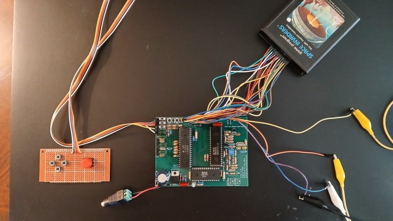
For as popular as Atari was in their heyday, it wasn’t until well after they were on their famous decline that they released their first handheld, the Atari Lynx. In retrospect, competing with the Game Boy was not going to be a recipe for success even without considering their other problems as a company, and as a result was their penultimate console before exiting the market completely. But [Nick]’s most recent project asks what the world would have been like with an Atari handheld from their golden era, and has been working on this miniaturized version of the 2600.

Unlike any modern emulators which can easily handle Atari 2600 games in almost any form factor today, this console is doing it all with as much original hardware as possible. It uses much smaller switches and buttons compared to the original, and omits some other unnecessary hardware for today’s world like the RF modulator. [Nick] has also designed a custom PCB that reduces the overall footprint considerably as well, and has relocated the cartridge port in preparation for its eventual handheld shape. The result is a console using original hardware that’s less than half the footprint of the original.

Although there were around 30 million Atari 2600 consoles sold and the system is unlikely to be a real collector’s item anytime soon, [Nick] makes sure to note that no real 2600 hardware was harmed in this build. And, as far as its handheld nature, this is a stepping stone on the path to that eventual goal. We’ll look forward to an eventual system that integrates a screen and controller as well as a port for the original cartridges. In the meantime, here’s another handheld 2600 that fits completely inside one of those cartridges.
Continue reading “Miniaturizing The Atari 2600 Console”

Flexible PCBs: Not Only For The Few

Flexible printed circuit boards are a fascinating technique for making electronics venture beyond the two-dimensional, but surprisingly they’re not something many of us have worked with. [Jessica Stanley] gave a talk at the recent Electromagnetic Field event in the UK, exploring the different ways to make your electronics bend.

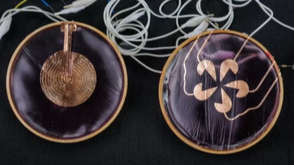
She starts with an overview of flexible electronics, detailing the techniques used with conventional polyimide substrates and etched copper.  We’re particularly enamoured of a stretchable PCB made by coiling a flexible circuit round a piece of elastic. Since she’s looking for techniques accessible to everyone that don’t either cost a fortune or require dangerous chemicals we look at conductive paint and electrolysis, before arriving at using a vinyl cutter to create adhesive traces.

We’ve no doubt all noticed that flexible PCBs can be ordered from the usual fabrication houses at a price, but the value in this talk lies in reminding the viewer that this is not the only path. She demonstrates well that simple flexible PCBs can be within the reach of almost anyone, which is perhaps the encouragement needed for people to try this medium. The full talk is below the break.

Continue reading “Flexible PCBs: Not Only For The Few”

Saving Some Coin With 3D Printed Stencils

One of the extra tools someone might need when working with surface-mount components is a solder paste stencil, which not only simplifies the application of solder paste to a PCB but increases accuracy. These metal stencils can cost an annoying amount of money and take time to get delivered, so this group has developed a method to 3D print them instead.

Starting with a PCB design in one’s tool of choice, the Gerber files can be sent to the online Stenchill tool to generate the stencil. Alternatively, a KiCad plugin exists as well. The tool will output files for a 3D printer from there. An FDM printer is required, with either PLA or PETG filament, and some configuration in the slicer is needed to get the accuracy required for a useful stencil. But once that’s all set up, the printer can output a perfectly usable stencil at a fraction of the cost, and without having to wait days for delivery through the mail.

It’s not all upside, though. Although it might be better than applying solder paste with a syringe on a massive board or doing more than one smaller board by hand, it may not be as good as a metal stencil for extremely small pads. But for those who often find themselves using metal stencils and dealing with the downsides that come with them, this could be a viable alternative, especially when prototyping.

If you have a laser cutter handy, that opens up some additional options for stencil production.

Continue reading “Saving Some Coin With 3D Printed Stencils”

PCBs Straight From The Magazine

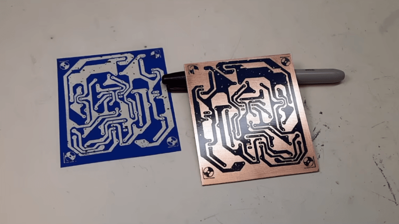
It’s never been easier to get a printed circuit board made. In fact, almost every electronics video out on the internet will incessantly remind you of this fact now. But making a custom PCB wasn’t always as straightforward as sending a KiCad file to a board house. Many DIY methods involve harsh chemicals and tedious processes, but did have the potential benefit of taking much less time than waiting on boards to arrive in the mail. [Bettina Neumryr] is demonstrating one of these older methods, called the toner transfer method, using a circuit that was printed directly in an old magazine.

The first part of the toner transfer method is to create an image that can be printed. Since this circuit came from a magazine, it is first scanned in to a computer and imported into GIMP, where it can be scaled to match the size of the components and then sharpened to make a crisp print. With the image ready, it’s time to print the image onto some toner transfer paper, ensuring that the printer in question is a laser printer which actually uses toner. From there, a sheet of blank copper PCB is prepared and then the toner is transferred by heating, in this case using a laminator. After that its etched, removing all of the copper not protected by the toner, and then the toner itself can be removed which leaves behind the copper traces.

For those of you who were around when toner transfer was in vogue, this video might not have much value. But for anyone who can’t use a board manufacturer for whatever reason or is looking for alternatives, a modern video showing the method could be much more useful and have better context for beginners than videos made a decade or more ago now. Some of those older methods include similar processes using inkjet printers instead, but there are more modern DIY methods as well using lasers or CNC machines too.

Continue reading “PCBs Straight From The Magazine”

DIY Ceramic Circuit Boards Surely Count As Solarpunk

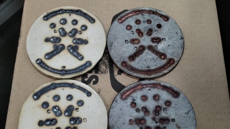
Solarpunk is all about combining that DIY hacker ethos with sustainability and renewable resources. Our usual PCB manufacturing methods, with their bevy of chemical baths and petrochemical resins aren’t exactly the most sustainable. Digging up some clay and firing it into a circuit board? Very sustainable! And apparently doable, as demonstrated by [Emily Velasco] on Mastadon.

Of course anybody could take a ceramic wafer and call it a circuit board, but that’s only part of what [Emily] did. The ceramic wafer is apparently native clay, which is very cool. Even cooler is that she’s baked the traces into the pottery. While you could conceivably use some sort of conductive glaze for this, what [Emily] did was stamp her desired circuit into the unfired ceramic using a 3D-printed stamp, and then fill the depression with copper powder after the first firing. After that, a second firing is done in a reducing atmosphere to melt/sinter the copper together–it’s not totally clear which is happening here–without burning up.

The results speak for themselves; on the finished demo board, a pair of LEDs blink happily away, driven by the astable oscillator circuit baked right into the clay– and of course the components soldered to it. You’ll have to click through to see it, though.

Given those not-so-sustainable petrochemicals behind our favourite PCBs may be in short supply, this is a timely hack. If it seems familiar, that’s because we featured virtually the same technique last year, but using more-expensive silver powder instead of copper, and a campfire instead of a kiln.

Thanks to [smellsofbikes] for the tip!

Slightly Sentient D20 Might Subtly Shift Your Rolls

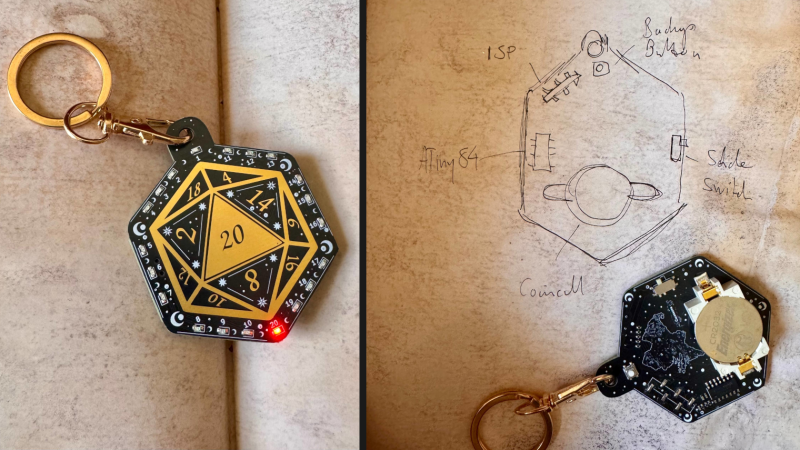
A twenty-sided die (d20) is a common thing in tabletop gaming, and [kati]’s slightly sentient d20 is a PCB that not only delivers random results on demand, but responds to hot and cold streaks and may even tweak the results a little to reflect its mood.

On its face the unit is a touch-sensitive PCB with twenty small charlieplexed LEDs around its perimeter, one for each die result. When activated by a touch on the center pad, the die dutifully animates a die roll and delivers a result. But something happens if the RNG (random number generator) coughs up results that are unusually lucky, or unlucky.

In addition to moods, there are reportedly other hidden features to discover.

After a streak of natural 1s, the device gets cranky. It begins to ignore the occasional activation input, and may glitch before a roll, reflecting a low mood. In addition, future rolls while in a low mood have a slight chance of being silently discarded and re-rolled into a low range (1-6), prolonging the unlucky streak. The inverse is true of a die that encounters a lucky run of natural 20s, with the die’s mood shifting to high spirits and having a slight chance of re-rolling future results into a high range (16-20).

The idea is to create (and feed) the feeling of lucky and unlucky streaks. Gamers are of course perfectly capable of projecting such feelings all on their own, which means the die acts as both mirror and amplifier of these emotions. In addition, each die acts slightly differently as a result of being imprinted with different RNG seeds, timing values, and response times which makes each one feel unique. There are reportedly other hidden features as well.

If you’d like to try making your own, keep an eye on the GitHub repository. The originals have design elements that were heavily personalized for [kati]’s gaming group, so the design files are in the process of being turned into a meaningful public release. Of course, there’s more than enough detail already to roll your own if you are so inclined.

PCB Map Display Keeps An Eye On Family

PCBs are traditionally designed with traces laid out to support a circuit full of electronic components. However, they’ve become increasingly popular as a way to produce functional visual artworks. This PCB map from [Jonathan] is a great example.

The PCB was designed as a map of the California East Bay area. The roads are laid out as the top-side copper layer, while the land and roads are used for the top solder mask layer, with the flipped land and roads area making up the solder mask on the bottom side. The map data itself was cribbed from Snazzy Maps. Behind the PCB, [Jonathan] mounted a 64 x 32 RGB LED array, which can be seen glowing through from behind the material. The LEDs are controlled by an ESP32, which grabs location data from [Jonathan’s] family member’s mobile devices over MQTT, and uses it to light their positions on the map. Files are on Github for the curious.

If you’ve got a family that is open to location tracking, and the money to pay for a custom PCB, you could probably recreate this project yourself. We’ve seen some other great PCB maps before, too, like this amazing metro tracker. Video after the break.
Continue reading “PCB Map Display Keeps An Eye On Family”