
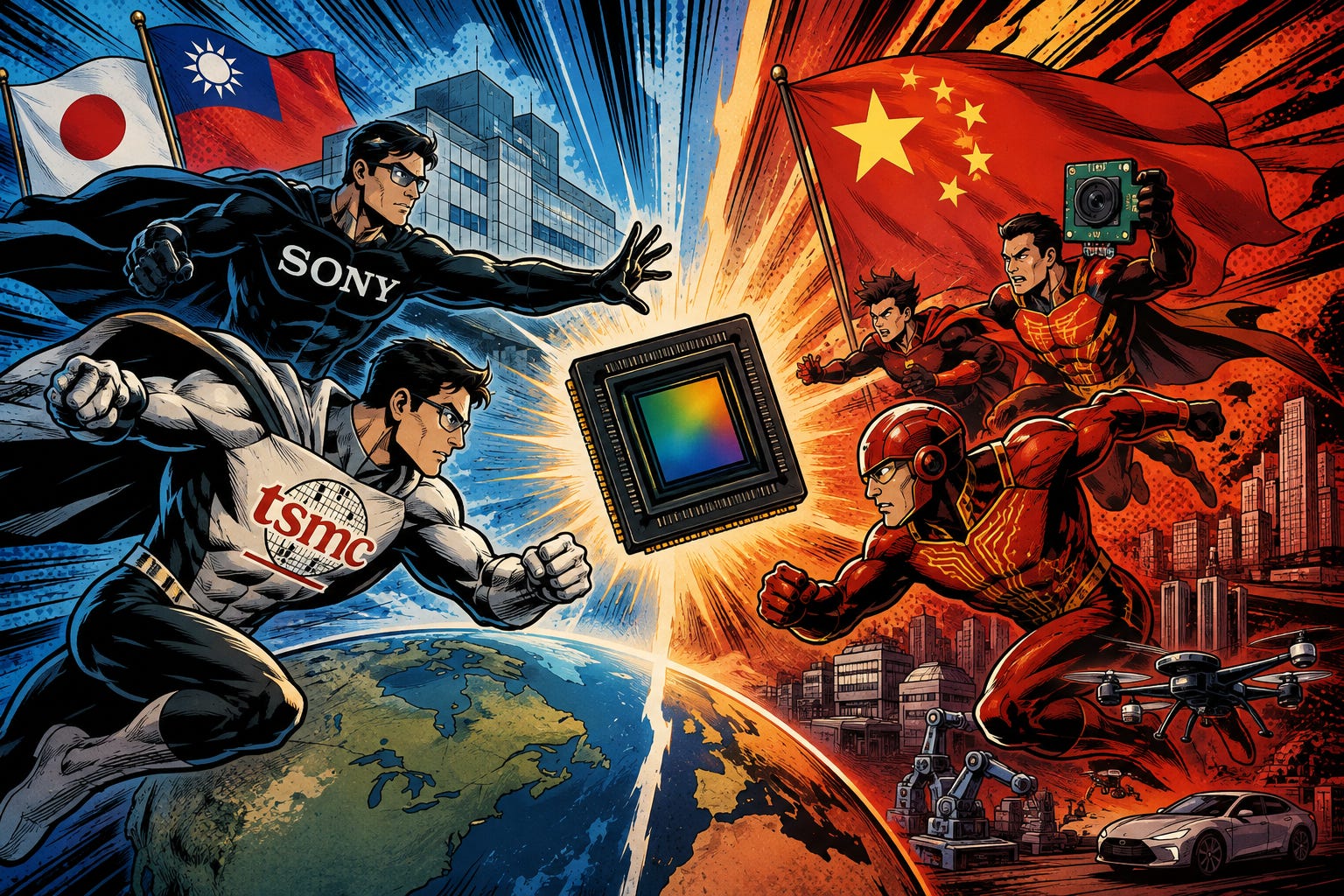
While almost every semiconductor discussion in 2026 has been dominated by AI GPUs, HBM, advanced packaging and data-center infrastructure, another strategically important semiconductor battle is moving rapidly into the foreground: the image sensor.
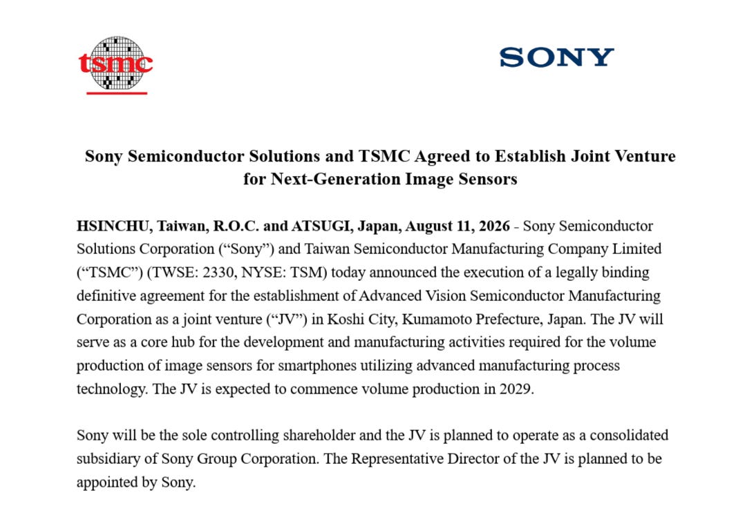
On August 11, Sony Semiconductor Solutions and TSMC signed a legally binding definitive agreement to establish Advanced Vision Semiconductor Manufacturing Corporation in Koshi City, Kumamoto Prefecture. The joint venture is scheduled to begin volume production in 2029 and will become a core development and manufacturing hub for next-generation smartphone image sensors using advanced process technologies.
Sony will remain the controlling shareholder and lead core sensor technology development, product planning and design. Sony plans to contribute approximately ¥465 billion, including cash and assets from its newly built Koshi fab, while TSMC plans to contribute approximately ¥282 billion in cash. The investments will be phased according to demand and business conditions.
This is therefore much more than another foundry agreement.
It represents a structural change in how the image-sensor industry may operate during the next decade.
Sony brings arguably the world’s strongest image-sensor product definition, pixel architecture and customer understanding. TSMC brings advanced logic processes, manufacturing discipline, yield management and a production ecosystem capable of translating increasingly complex semiconductor architectures into high-volume products.
Together, they are effectively creating a new industrial model for imaging:
sensor innovation led by the application company, logic manufacturing enabled by the world’s leading foundry, and production geographically anchored inside a strategically supported Japanese semiconductor cluster.
And behind the deal is an even larger story.
The global CIS industry is beginning to split into competing—and sometimes overlapping—technology ecosystems centered on Japan, Taiwan, China and U.S.-controlled computing platforms.
Traditionally, CMOS image-sensor competition was relatively straightforward.
The industry competed on pixel size, resolution, sensitivity, dynamic range, low-light performance, power consumption and manufacturing cost.
That model is changing.
A smartphone camera is no longer simply capturing an image and sending it to an application processor. Modern imaging systems increasingly combine multiple exposures, multiple cameras, depth information, motion sensing and machine-learning algorithms before the user even sees the final image.
The next step is even more important.
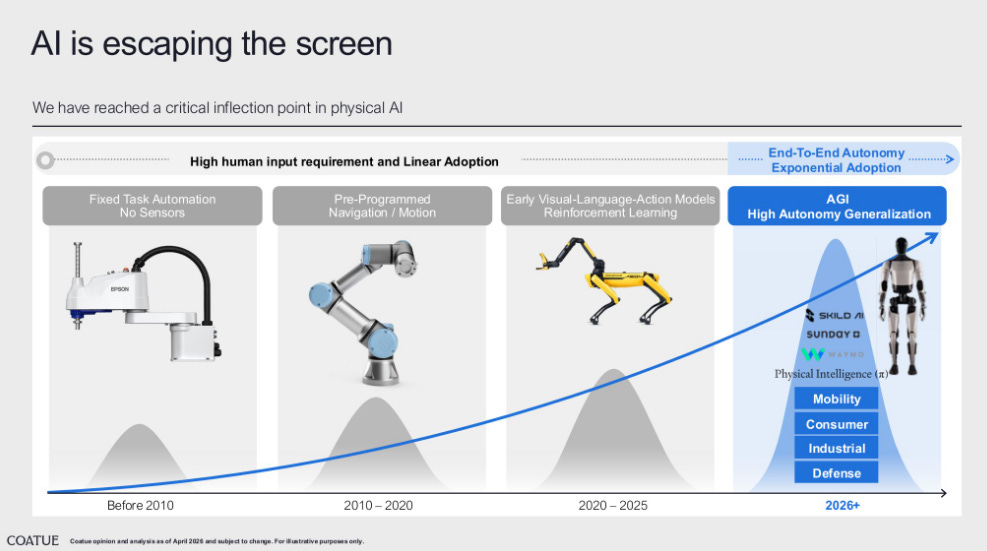
As AI moves from cloud-based language models toward on-device AI, robotics, autonomous vehicles, industrial machines and spatial computing, the sensor itself becomes part of the computing architecture.
The camera is becoming the front-end processor of the physical world.
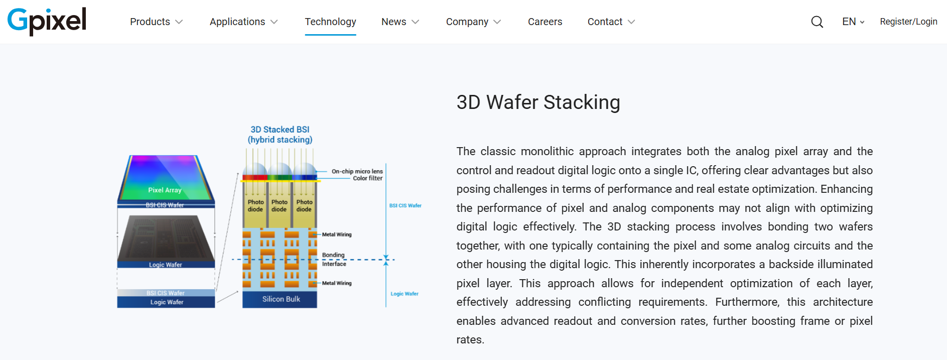
That requires increasingly sophisticated stacked architectures: a highly optimized pixel layer for photon capture combined with increasingly capable logic underneath it for readout, signal processing, memory management and potentially AI acceleration.
Sony has already pushed aggressively into stacked CIS architectures. TSMC’s participation suggests that the distinction between a traditional CMOS sensor and an advanced heterogeneous computing device will continue to blur.
The manufacturing requirements begin to resemble some of the challenges appearing elsewhere in advanced semiconductors: finer interconnects, more complex wafer stacking, higher bandwidth between functional layers, increasingly sophisticated bonding and tighter co-optimization between design and manufacturing.
In other words, advanced packaging concepts are gradually entering the imaging world as well.
The location may be almost as important as the technology.
Kumamoto has already become the symbolic center of Japan’s semiconductor revival through TSMC’s JASM investments. Sony’s existing image-sensor manufacturing footprint makes the region even more strategically significant.
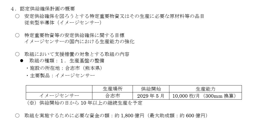
Japan’s Ministry of Economy, Trade and Industry had already approved Sony’s Koshi image-sensor project under Japan’s economic-security framework in April 2026. The approved plan targeted approximately 10,000 300mm-equivalent wafers per month, with supply beginning around May 2029 and production expected to continue for at least ten years. METI said subsidies could reach ¥60 billion.
This makes the policy intention unusually clear.
Japan does not view image sensors merely as consumer-electronics components. METI explicitly described them as the electronic eyes required for autonomous driving and physical AI.
The strategy therefore stretches far beyond smartphones.
Japan is assembling a semiconductor ecosystem that combines logic manufacturing, sensors, materials, equipment, automotive electronics and eventually physical-AI applications.
The Sony-TSMC joint venture turns Kumamoto from simply another wafer-production location into something closer to an integrated semiconductor technology cluster.
And the timing matters.
On the same day the Sony partnership was finalized, TSMC’s board approved another US$29.4425 billion capital budget covering advanced process capacity, advanced packaging, mature and specialty technologies, fabs and infrastructure. The board also formally approved investment of up to ¥282 billion in the Sony joint venture.
Seen in that context, image sensors are not a side project.
They are becoming another extension of TSMC’s manufacturing platform.
The first-order beneficiaries are obvious: Sony and TSMC.
But the more interesting opportunities may appear one or two layers further down the supply chain.
A more sophisticated stacked image sensor requires significantly more than front-end wafer fabrication.
It creates demand for technologies associated with:
wafer-to-wafer bonding, hybrid bonding, wafer thinning, temporary bonding and debonding, backside processing, CMP, advanced lithography, precision metrology, wafer inspection, dicing, test and highly controlled contamination management.
Japan is particularly well positioned here because its semiconductor strength is unusually concentrated in materials, manufacturing equipment and precision processing technologies.
Companies across photoresists, silicon wafers, CMP materials, bonding materials, inspection, deposition, cleaning, dicing and test could therefore participate indirectly as the Kumamoto ecosystem expands.
But one distinction is important for investors: not every supplier in the Japanese semiconductor ecosystem automatically becomes a beneficiary.
The key questions will be which process steps Sony and TSMC internalize, which tools are qualified for the new architecture and whether critical packaging or stacking operations remain in Japan or are distributed across existing Sony and TSMC facilities.
Those qualification announcements may ultimately be more useful investment signals than the headline fab announcement itself.
Sony’s biggest immediate battlefield remains premium smartphones.
Yole Group estimated that Sony represented close to 50% of global CIS revenue in 2025, with its position supported by premium mobile imaging, larger optical formats and advanced stacked architectures. In mobile specifically, Yole estimated Sony’s share at approximately 57%.
That explains why the partnership matters strategically.
As flagship smartphones become increasingly homogeneous in CPU performance, displays and memory, camera capability remains one of the clearest ways manufacturers can differentiate devices to consumers.
But the camera competition is shifting.
Future differentiation may come not simply from larger sensors or more megapixels, but from tighter integration between the sensor, ISP, application processor and AI software.
That favors suppliers capable of coordinating multiple layers of semiconductor technology simultaneously.
Sony plus TSMC therefore creates a formidable combination.
The consequence will propagate through the smartphone imaging ecosystem: camera-module makers, lens suppliers, autofocus and stabilization components, packaging providers, testing companies and optical-material suppliers will all face increasingly demanding specifications.
This is where the geopolitical story becomes much more interesting.
For years, the simplified industry narrative was that Sony dominated premium sensors, Samsung challenged Sony in smartphones, while Chinese CIS companies competed primarily through price and domestic substitution.
That description is becoming outdated.
According to industry analysis, China became the world’s second-largest CIS supplier base in 2025, overtaking South Korea, driven by companies including OmniVision, SmartSens, GalaxyCore and Gpixel.
This is a major structural development.
Chinese CIS companies are benefiting from one of the world’s largest domestic ecosystems for smartphones, surveillance systems, EVs, drones, robotics, AIoT devices and smart-home products.
That means China possesses something extraordinarily valuable for semiconductor development:
A massive internal application market capable of generating both volume and rapid product iteration.
The competitive challenge is therefore not simply whether Chinese companies can reproduce an existing Sony sensor.
The bigger question is whether Chinese sensor suppliers can use China’s enormous downstream electronics ecosystem to shorten the feedback loop between sensor design, systems integration and commercialization.
That is exactly how semiconductor ecosystems become dangerous competitors.
One transaction illustrates this shift particularly well.
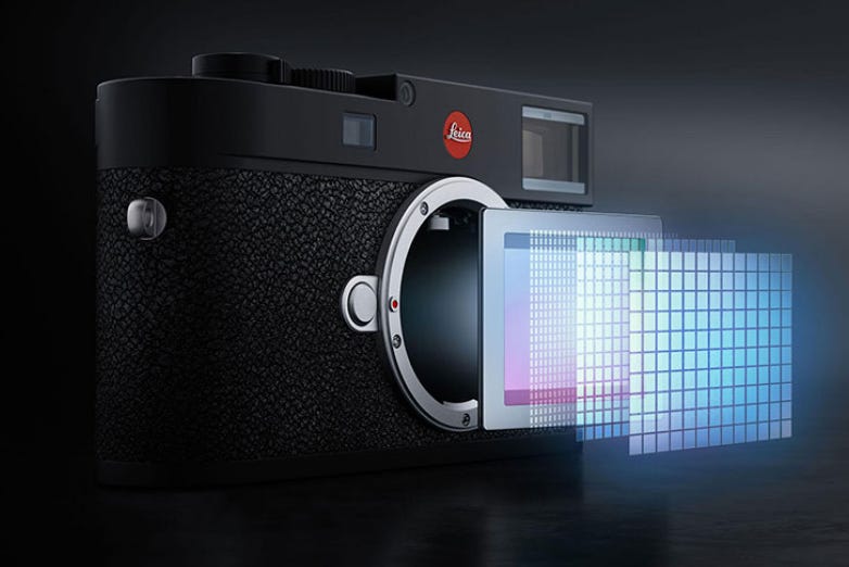
On April 20, 2026, German premium camera manufacturer Leica Camera AG announced a strategic partnership with China’s Gpixel to jointly develop a high-performance CMOS sensor specifically tailored for future Leica cameras.
This is not simply an off-the-shelf component procurement agreement.
Leica and Gpixel said they will cooperate on sensor engineering, validation, image tuning and production readiness, with engineering resources spanning Wetzlar, Antwerp and Changchun.
That matters.
Leica is one of the strongest premium imaging brands in the world. A company operating at that level choosing to co-develop a bespoke sensor with a Chinese CIS supplier is an indication that Chinese image-sensor companies are beginning to compete for technology credibility, not merely volume.
Gpixel’s historical strength has been in industrial, scientific and professional imaging rather than mass-market smartphones. That may actually make the Leica partnership more strategically interesting because advanced industrial imaging requires expertise in areas such as high dynamic range, low noise, high-speed readout and specialized sensor architectures.
The Sony-TSMC and Leica-Gpixel announcements therefore form an interesting pair.
One strengthens a Japan-Taiwan advanced manufacturing alliance.
The other demonstrates that a Chinese CIS supplier can penetrate a premium European imaging platform.
The global imaging supply chain is not simply decoupling.
It is reorganizing into multiple centers of technical competence.
The U.S. angle is different.
America does not currently dominate merchant CMOS image sensors in the same way it dominates GPUs or certain parts of semiconductor equipment and EDA.
Instead, U.S. influence sits primarily at the system and computing-platform layers.
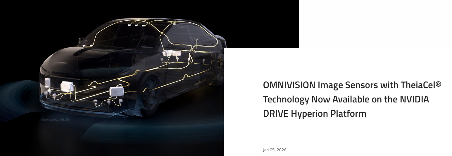
Apple is one of the major drivers of premium mobile imaging demand. NVIDIA increasingly defines computing architectures for autonomous vehicles and robotics. For example, OmniVision’s automotive sensors are already supported on NVIDIA’s DRIVE AGX Hyperion platform.
At the same time, U.S. semiconductor export policy continues to restrict China’s access to selected advanced computing technologies and semiconductor-manufacturing capabilities, even though CMOS image sensors themselves are not currently treated exactly like leading AI accelerators. BIS continues to maintain dedicated controls around advanced computing and semiconductor-manufacturing items, while its 2026 policy revisions show that access to powerful processors remains explicitly conditioned by national-security considerations.
This creates an important strategic consequence.
As restrictions make it harder for China to compete at certain parts of the leading-edge AI compute stack, Beijing and Chinese industry have even stronger incentives to build technological strength in areas where domestic markets can support scale.
Sensors are one of those areas.
Automotive semiconductors are another.
Power electronics, robotics, industrial control and mature-node analog chips are others.
The future U.S.-China semiconductor competition may therefore become much broader than a race over GPUs.
It may become a race to control the entire physical-AI value chain:
Sensor → connectivity → memory → compute → software → actuator.
This is why the long-term implications of the Sony-TSMC partnership may extend well beyond smartphone cameras.
Sony itself is already moving deeper into AI vision. In July 2026, Sony Semiconductor Solutions and Mitsubishi Electric announced plans for a separate joint venture developing AI vision-sensor solutions for manufacturing applications—another sign that Sony increasingly sees sensing as part of machine intelligence rather than simply digital photography.
That direction is logical.
Large language models taught machines to understand human language.
The next industrial transformation will require machines to understand the physical world.
Robots need cameras.
Autonomous vehicles need cameras.
Factories need cameras.
Drones need cameras.
AR glasses need cameras.
AI agents operating in physical environments need continuous streams of visual information.
Before AI can reason about the physical world, something has to capture it.
That makes the image sensor one of the most strategically important entry points into physical AI.
The financial contribution from the Sony-TSMC joint venture will not materially change the semiconductor industry’s 2026 earnings cycle.
Its strategic significance is much larger.
The deal reveals how the next phase of semiconductor competition is evolving.
The first wave of the AI semiconductor boom was about securing GPUs.
The second was about securing HBM and advanced packaging.
The next phase is increasingly about controlling the complete architecture connecting the physical world to AI computing.
Sensors capture reality.
Connectivity transports the data.
Memory stores it.
Processors interpret it.
Advanced packaging integrates the system.
AI software makes the decision.
Seen from this perspective, the Sony-TSMC partnership is not simply another Japanese semiconductor investment.
It is part of a much broader reorganization of the global technology supply chain.
Japan is attempting to anchor strategic sensor production domestically.
Taiwan is exporting advanced manufacturing capability into allied industrial clusters.
China is building an increasingly competitive domestic CIS ecosystem and is beginning to win credibility in higher-end applications.
And U.S. technology platforms continue to shape the computing architectures into which those sensors ultimately connect.
The world is therefore not moving toward a single vertically integrated semiconductor supply chain.
It is moving toward multiple competing technology ecosystems connected by selective interdependence.
That distinction matters.
The Leica-Gpixel partnership demonstrates that premium Western companies can still choose Chinese semiconductor technology when performance and customization make commercial sense. The Sony-TSMC partnership simultaneously demonstrates that governments and major semiconductor companies are willing to invest billions to geographically secure strategically important production.
Both trends can exist at the same time.
And that may be the defining characteristic of the semiconductor industry over the next decade.
The battle is no longer only about who builds the fastest AI processor.
It is increasingly about who controls the technologies that allow machines to see, understand and interact with the real world.
TSMC and Sony are now placing a very large bet on who will manufacture those eyes.
Comments
Nothing yet. Say the first thing.
Sign in to join the conversation.