
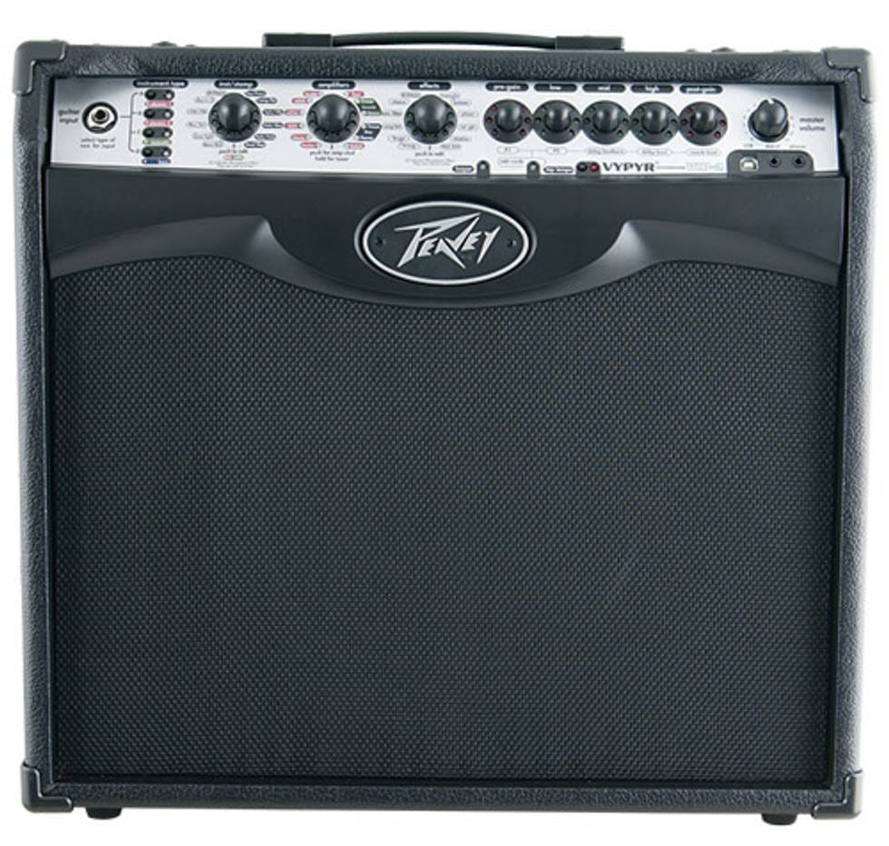
This is a continuation of investigations that commenced in this thread. I have moved the content here as the platform prevented sharing of some schematic document links (instant removal by moderators with no explanation). It is not intended to be a repair guide; more a collation of resources both found and generated to assist anyone needing to troubleshoot their devices. It also serves as a cautionary tail on some potential design flaws discovered during the proverbial troubleshooting goose chase.
The issue summary observed by forum user SolitaryMassacre is that the audio output from the amplifier is polluted by a 3kHz tone. Initially SolitaryMassacre’s suspicion was that the 1.2V core regulator (Diodes AP7361ADJ) for the ADSP-21375 was to blame, as a large 700mVpk-pk ripple was being observed on its input.
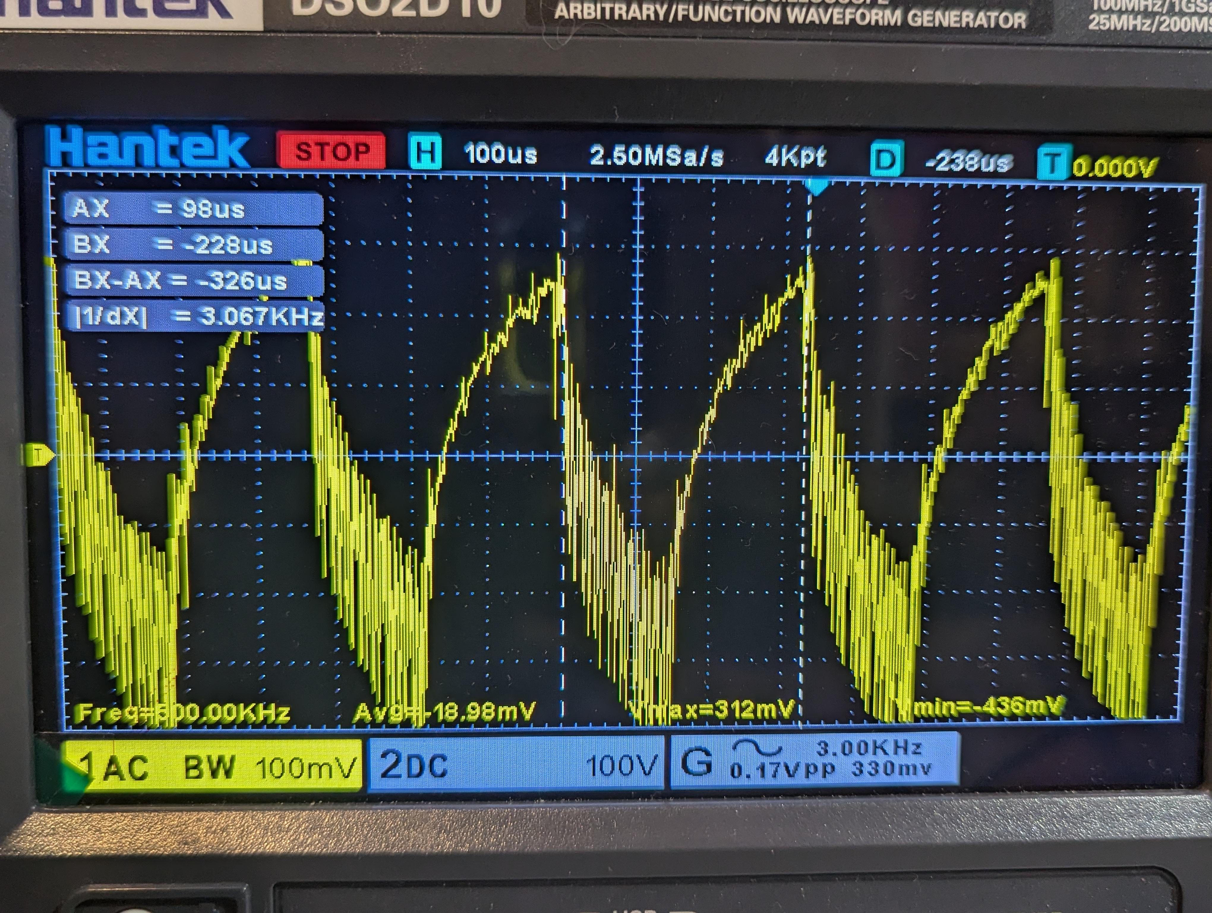
However upon looking at the series of four 1.3 Ohm resistors in front of the regulator, it quickly became apparent that this was likely expected behaviour.
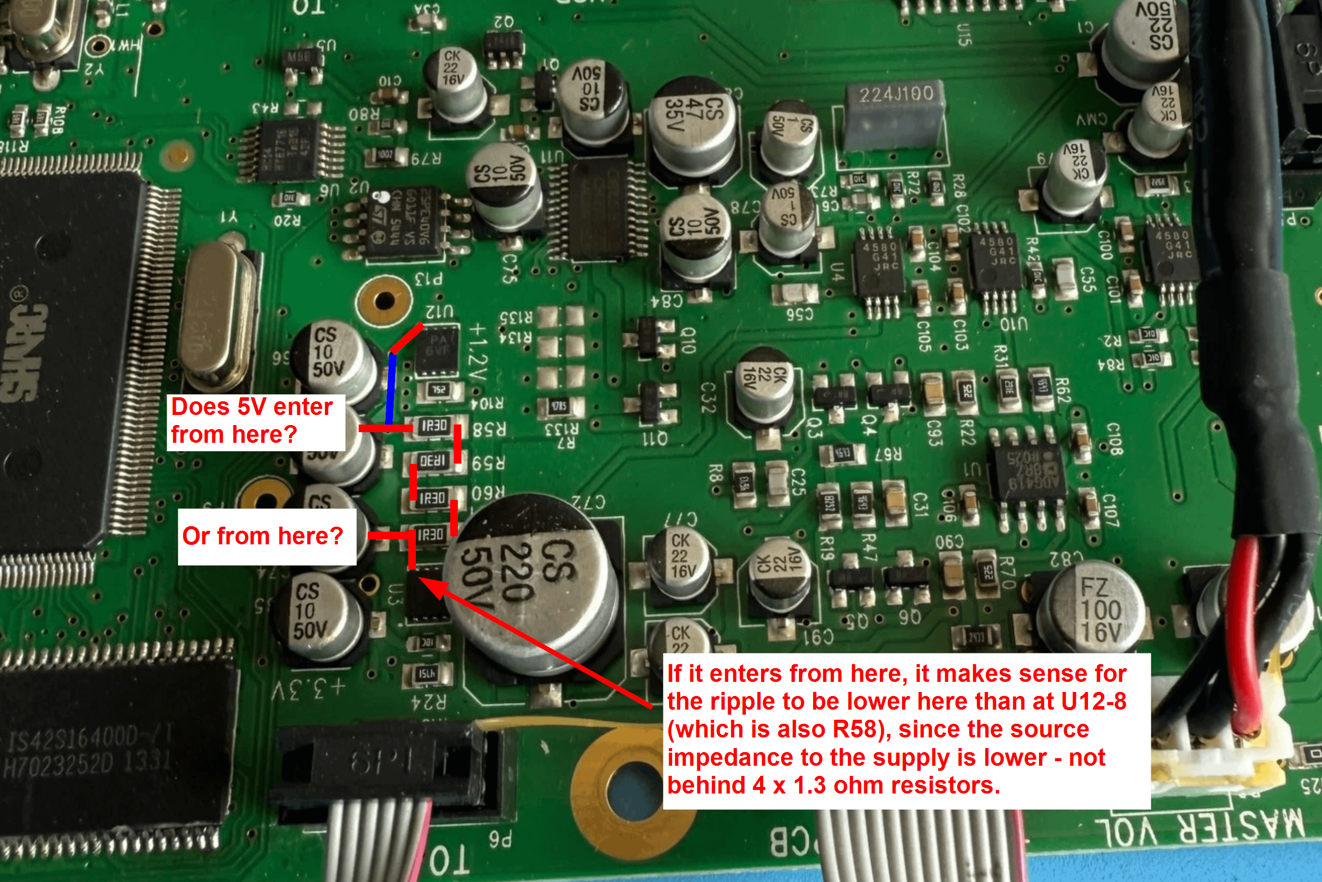
The core supply of the ADSP-21375 has a typical consumption of 600mA at 1.2V.

This means 3.12V average dropped across those four 1.3 Ohm resistors at full current. These resistors are also 1206, which are typically 1/4W, though there are some that go up to 1/2W. That would make for 1 ~ 2W of total power dissipation allowance. 3.12V across 5.2 Ohms results in 1.872W of power dissipated, or ~0.468W per resistor (note that per the schematics attached further down, these resistors are only rated to 1/4W - undersized). The resistor chain looks like it’s intended to relieve some of the dissipation burden from the AP7361. Without the resistors, the LDO would need to drop 5 - 1.2 = 3.8V, which at 0.6A, means 2.28W dissipated. The DFN8 is only rated to 1.7W, and its thermal resistance is 70C/W. 2.28W would therefore result in a 160C temperature rise - obviously not acceptable.
With the resistors inline, the average voltage at the regulator input with a 600mA load drops from 5V to 1.88V. The LDO now only needs to drop the remaining 0.68V, which at 600mA results in 408mW dissipated. Much more reasonable. Now the temperature rise at maximum load is only 28.56C.
Later on in the thread, TEV was able to locate partial schematics (one of the links that were removed by moderators) for the previous model (Vypyr 1) of the DSP board, which essentially confirmed this:
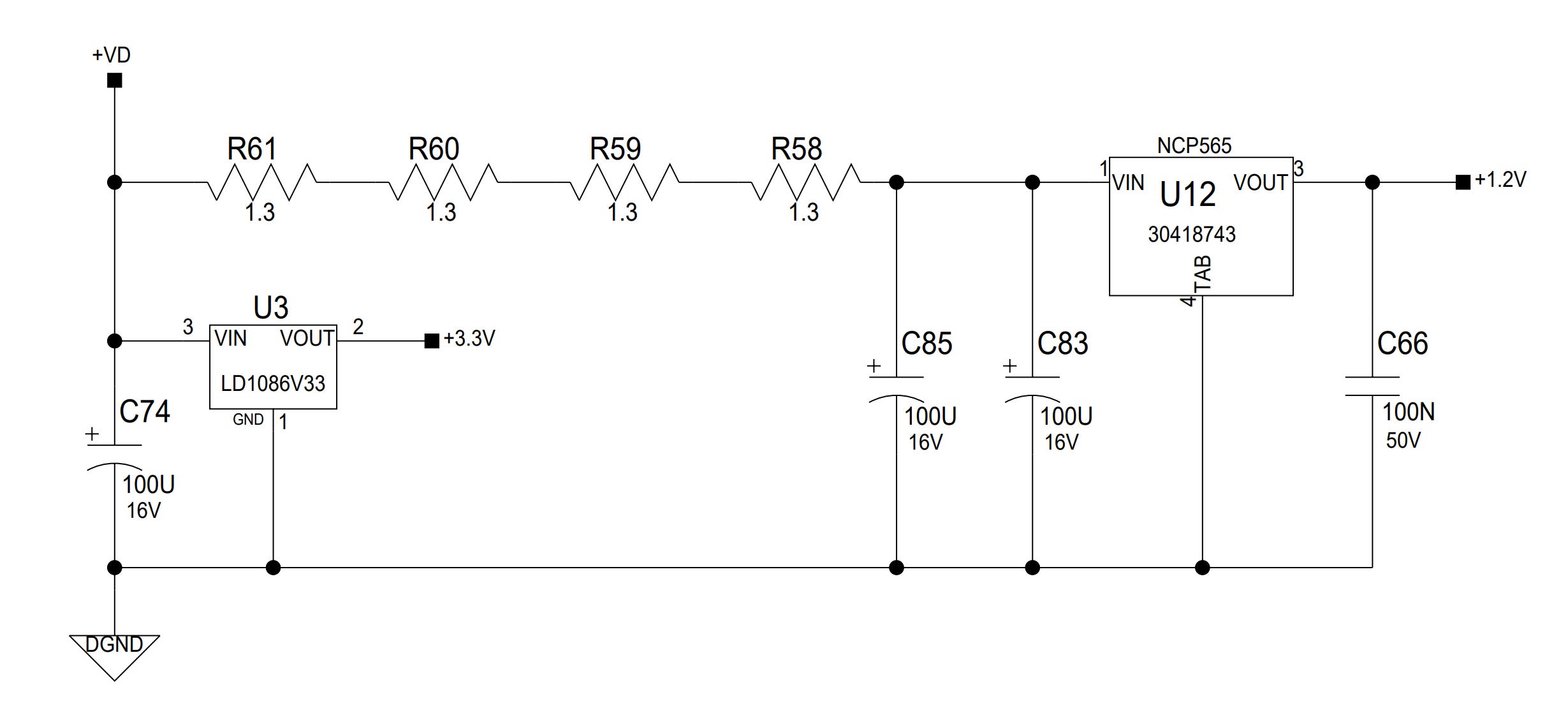
In short, this core rail current dependent ripple on the 1.2V LDO input is expected, as the drop (ripple) across the resistor chain will vary with said current. So the question isn’t why there is a voltage ripple on the LDO input, but rather why is the load current of the DSP core seemingly varying at 3kHz, and hence showing up as voltage ripple across the resistor chain and on the +VD rail?
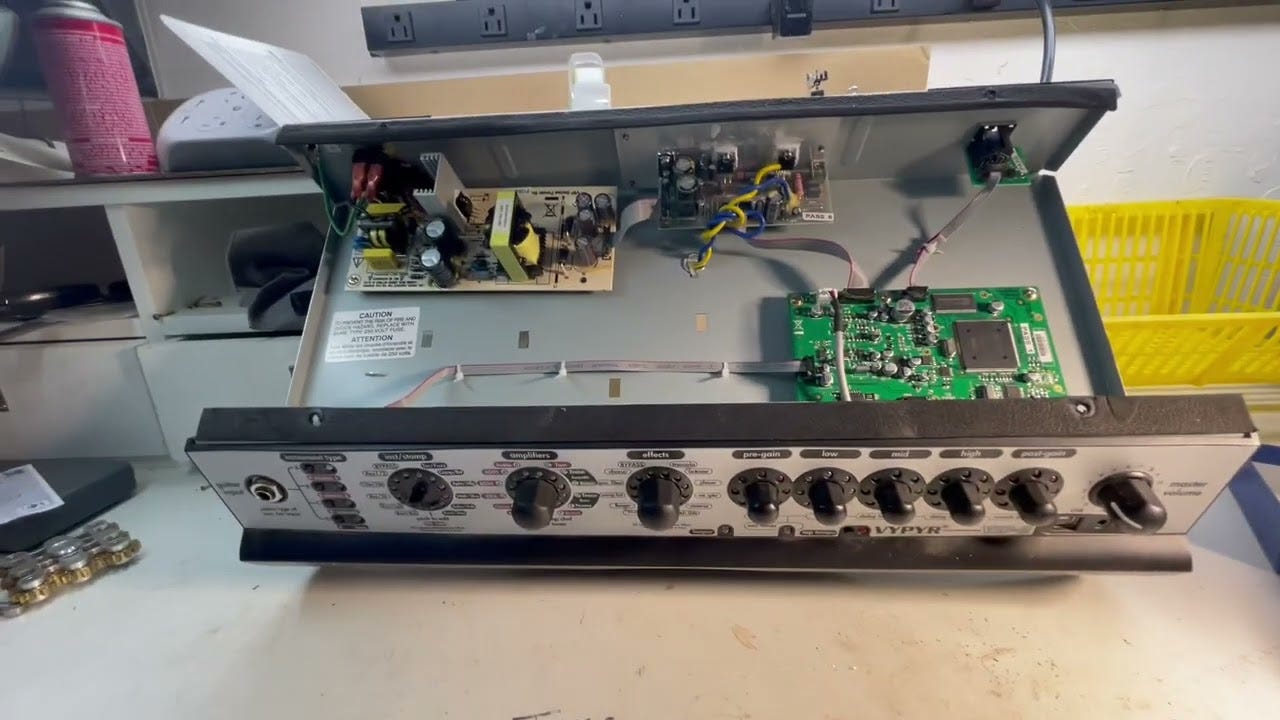
The amplifier comprises five boards:
Power Board
Amplifier Board
MIDI connector board
DSP board
Front Panel Board
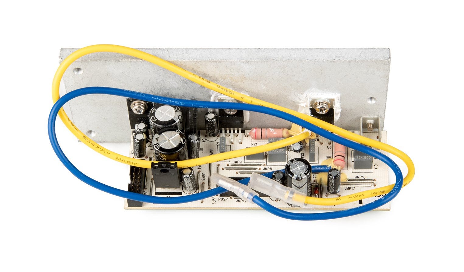
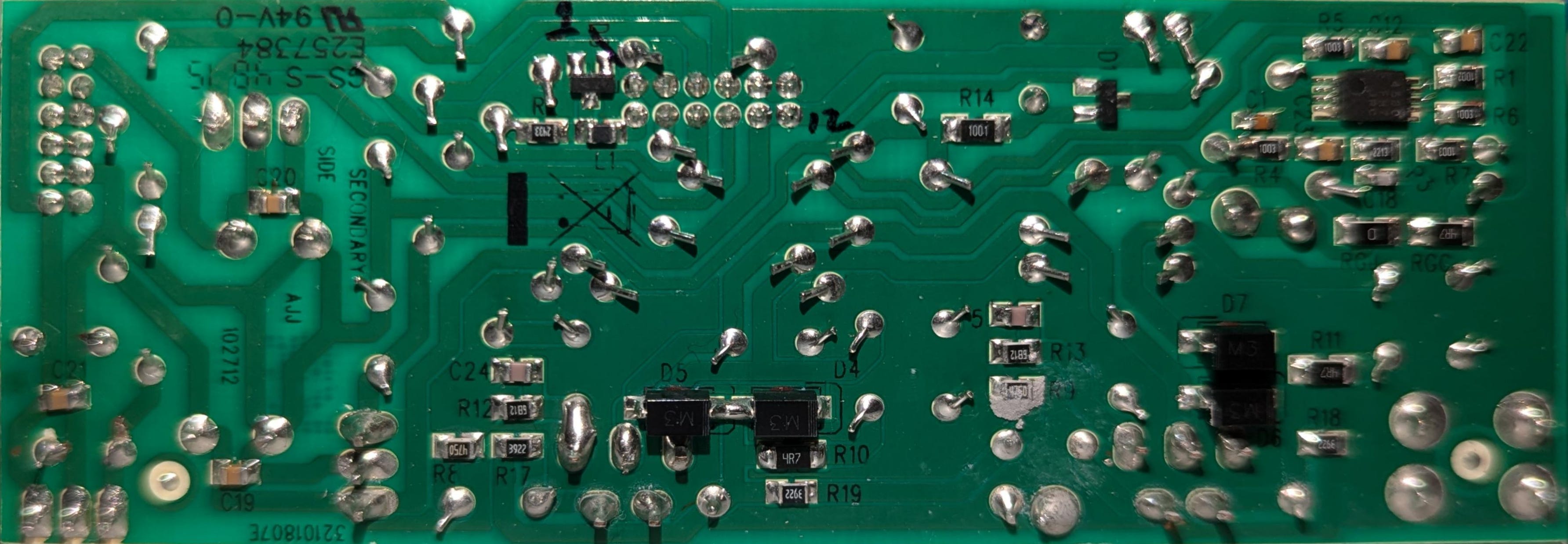
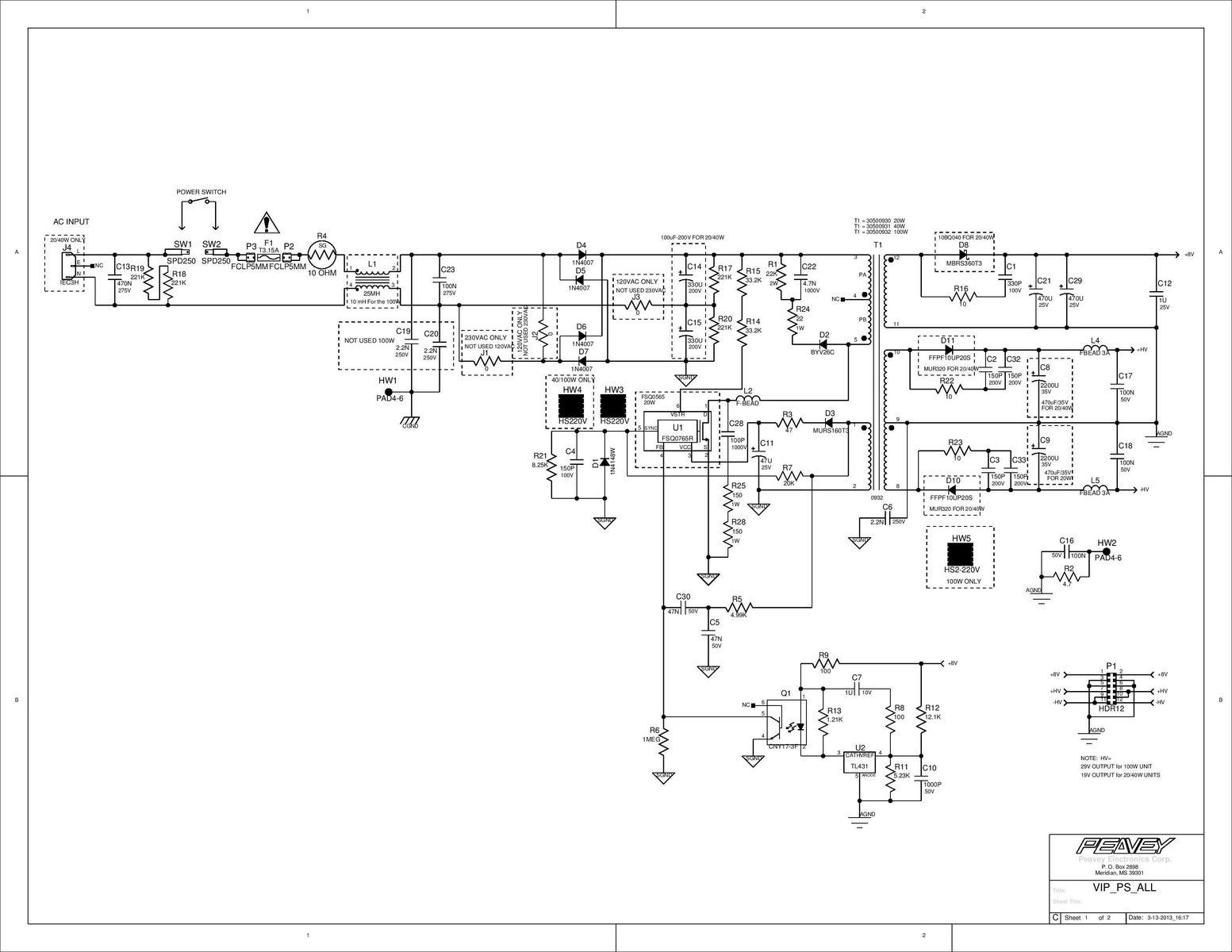
The schematics for most of these were also located alongside the DSP. These are attached below (the power board is an image). The power amplifier board schematics could not be found, however a basic board map (viewed from the bottom side) was put together in lieu of them.
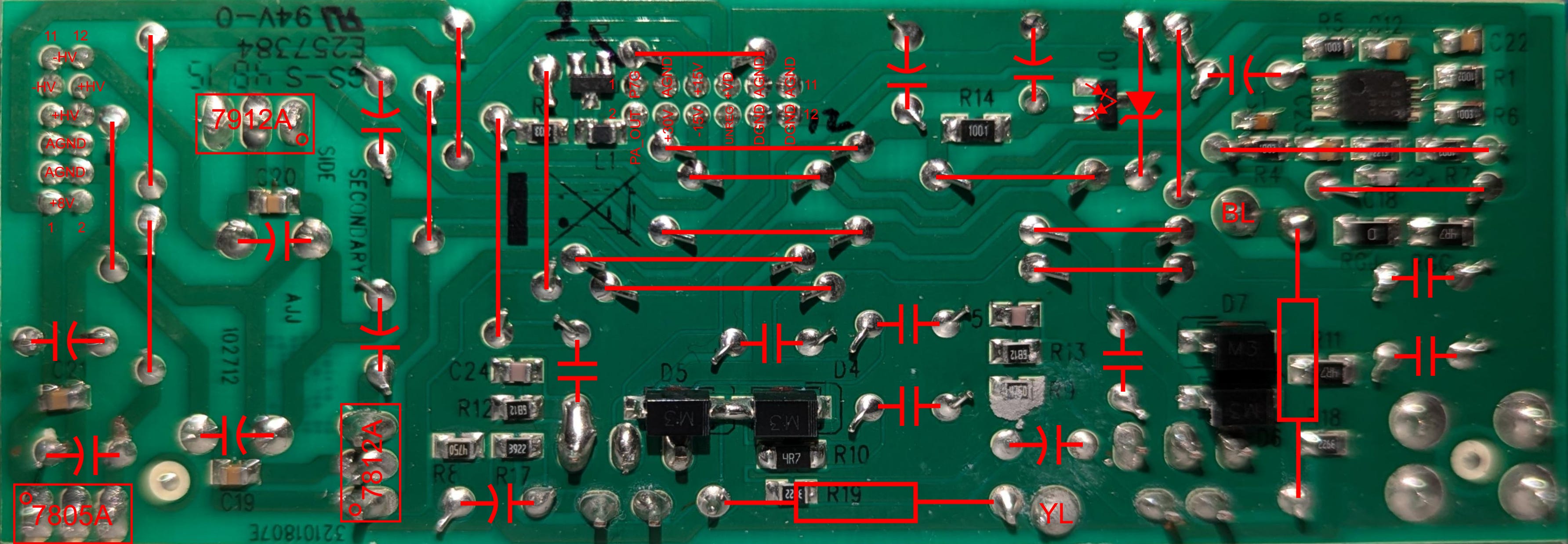
Based off these schematics, a basic power tree can be assembled:
Below are the three main rails that are generated by the power board, and all the regulated rails derived off them.
+8V
+VD
+3.3V
+1.2V
UNREG
+HV
+15V/+12V
HP+
-HV
-15V/-12V
HP-
Note the +/-15V rails will be +/-12V in the 20W and 40W variants of the amplifier.
+1.2V is only used for supplying the ADSP-21375 core rail.
+3.3V supplies the ADSP-21375 I/O rail, the SDRAM, the DSP configuration flash memory, the CS4270 I/O rail, a 74HC14 Schmitt trigger used on various logic-level lines throughout the DSP board, and the logic supply for the ADG419 analog switch used in the TransTube circuit. It also supplies power to the front panel board. The +3.3VD and +3.3VA are derived rails for powering the TAS1020B USB interface.
The +/-15V rails supply all the op-amps on the input and output of the CS4270, as well as the VDD and VSS rails for the ADG419 analog switch used in the TransTube circuit. The derived HP+/- rails supply the headphone power amplifiers. Additionally, a +5V analog supply for the CS4270 is derived from the +15V rail via a TL431-based discrete LDO circuit (Q1, Q2).
The outline below is annotated with probe points for all rails on the DSP board.
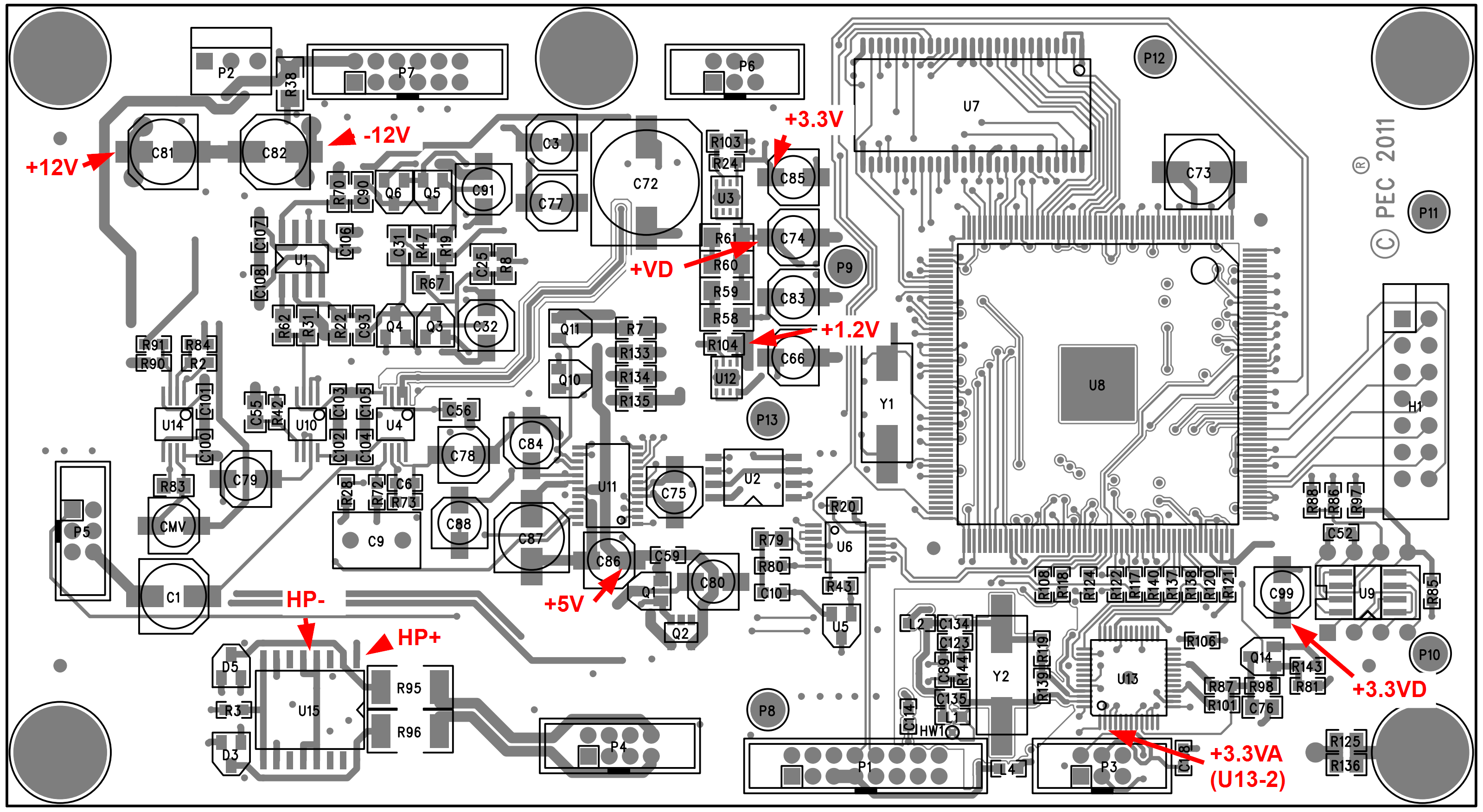
The DSP board maintains two grounds - AGND and DGND, which are connected at R7 through 47.5 Ohms. This resistance however becomes bypassed once the board is assembled into the chassis, as all of the mounting holes are connected to the common chassis GND.
Additionally, there is an error on the schematic compared to the production board. R125 and R136 claim to connect the mounting holes nearest them to DGND.
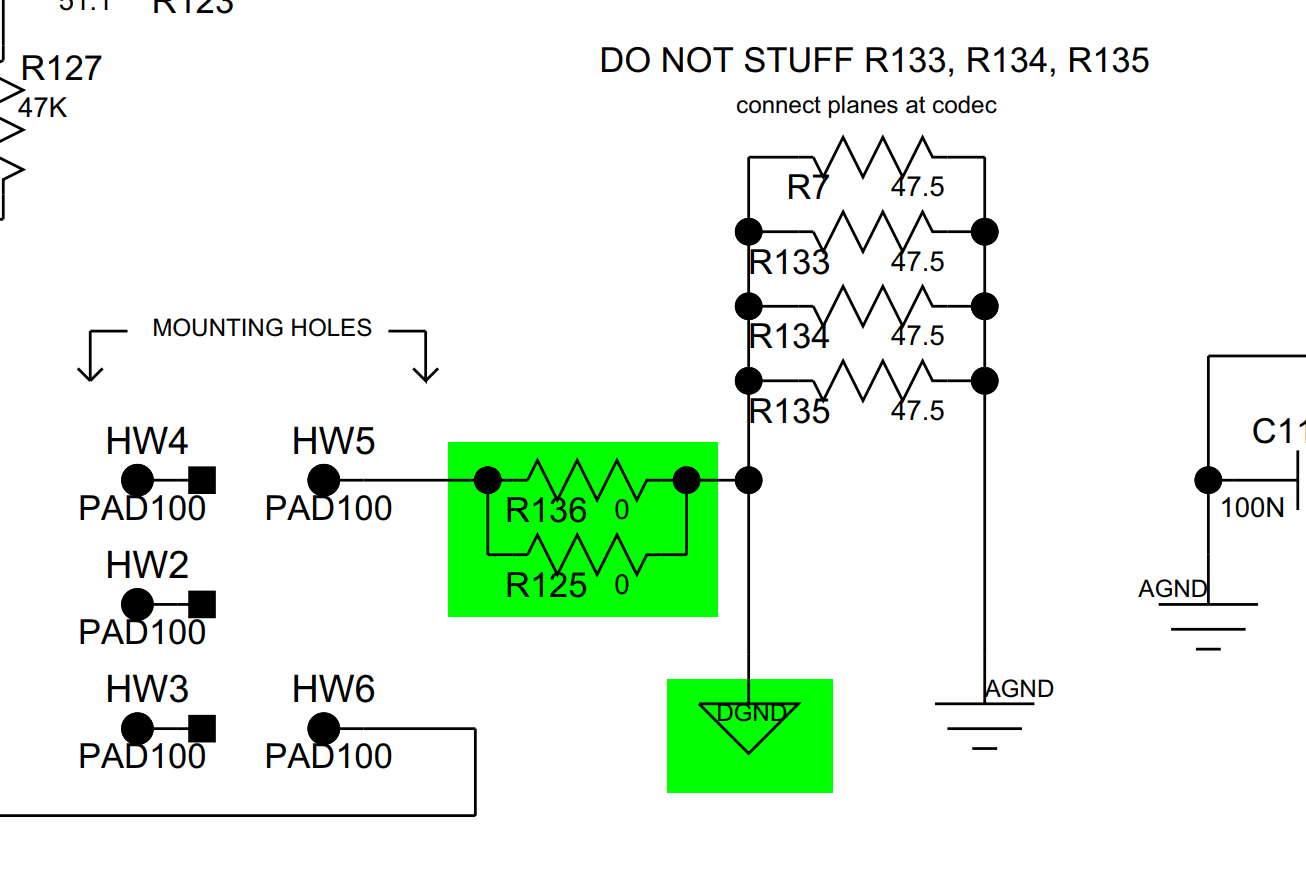
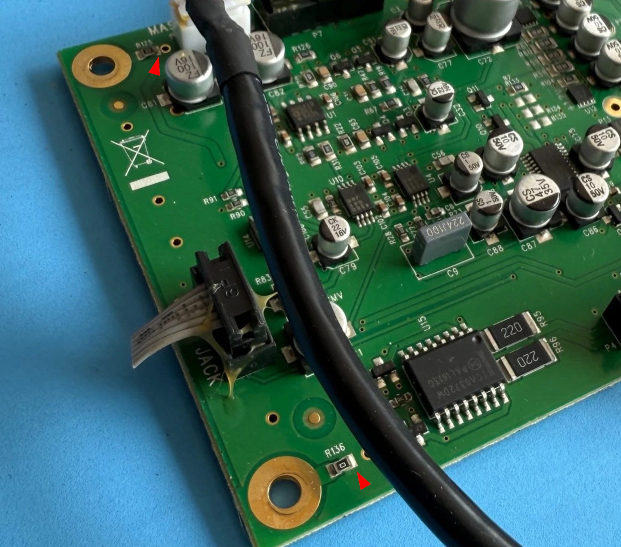
However when inspecting the above board photo, it’s clear that at least R136 connects to the polygon pour surrounding it, which has continuity to P7-9 and P7-11 (AGND).
Furthermore, there is another conflict in ground naming between the power and amplifier boards. The power board schematic clearly defines all grounds (P1-3,4,5,6) as AGND. However when connected to the amplifier board, following the AGND trace from the power supply connector (shown in green below) clearly shows it routes through DGND pins on the PDSP connector (pins 10 and 12).
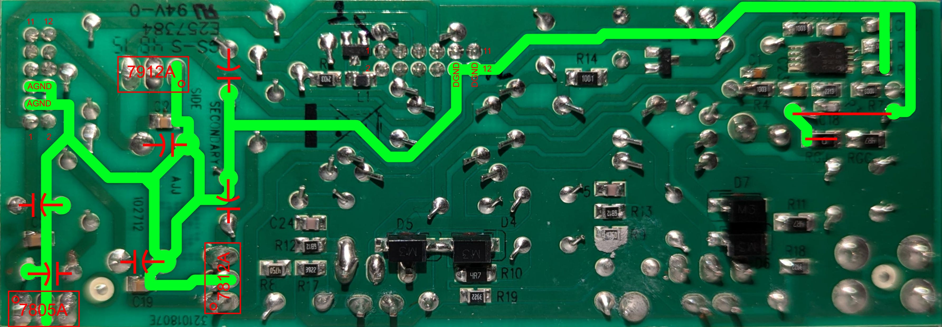
The likely suspects in most cases for power supply noise issues are degrading electrolytics. There are two suspect boards; the power board and the amplifier board, since they both handle regulation. As discovered in the power tree, there are only three rails that go from the power board to the amplifier board; +8V and +/-HV. These get linearly regulated by the amplifier board to +5V (+VD rail) and +/-15V (+/-12V for the lower power variants), before being output to the DSP board. Thus, to be able to power the DSP board entirely off bench supplies, we need only connect +VD and +/-15V (+/-12V) as follows:
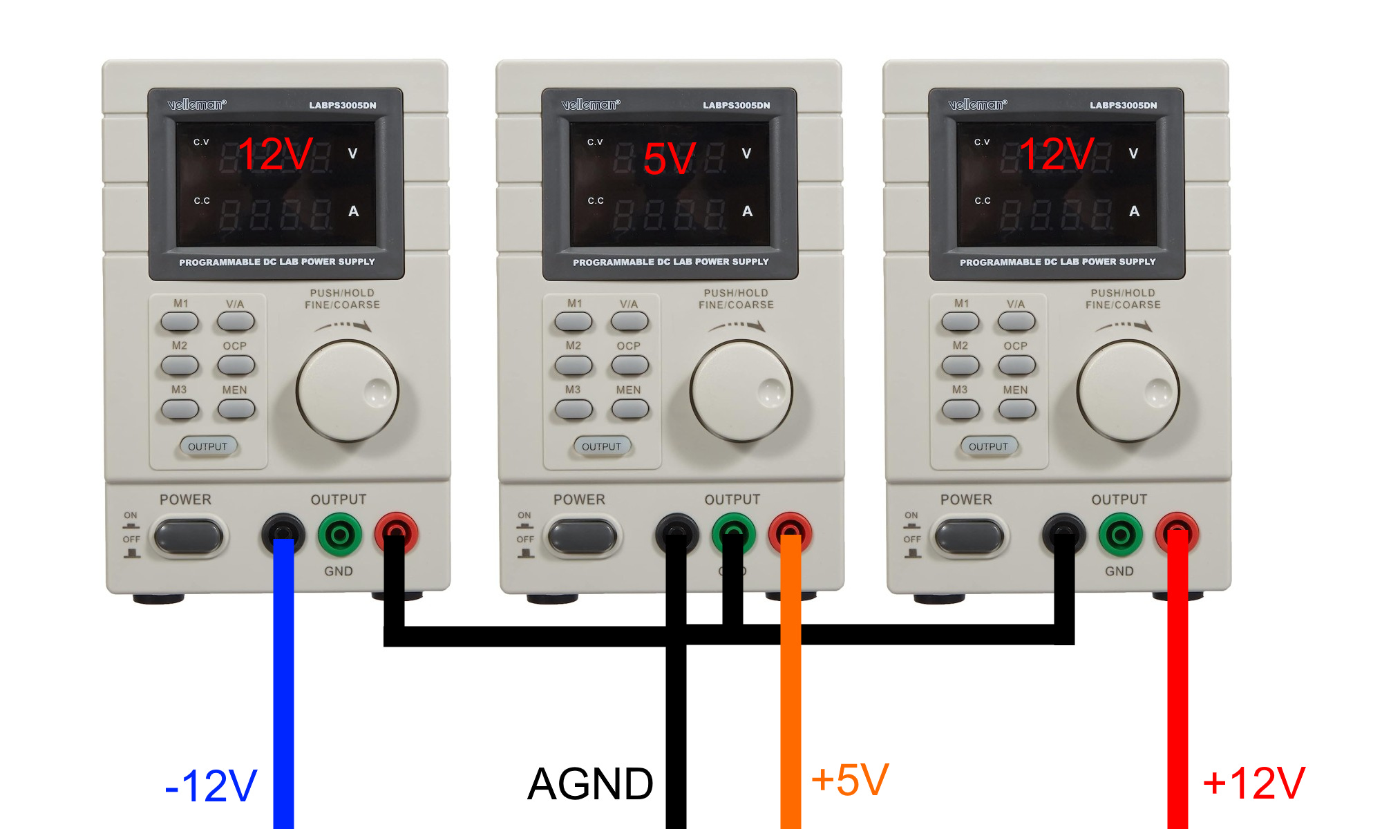
Doing so on SolitaryMassacre’s unit resulted in the noise persisting on the +VD rail. This essentially exonerates both the power board and the amplifier board of any fault. If this was switching noise from the mains stepdown transformer propagating through to the DC rails due to failing electrolytic capacitors, we would expect the issue to resolve when running entirely off bench power.
One other observation was made by SolitaryMassacre while probing around the SDRAM pins. The sawtooth waveform on the +1.2V and to a lesser extent the +3.3V rails correlated almost perfectly with SDRAM read/write activity.
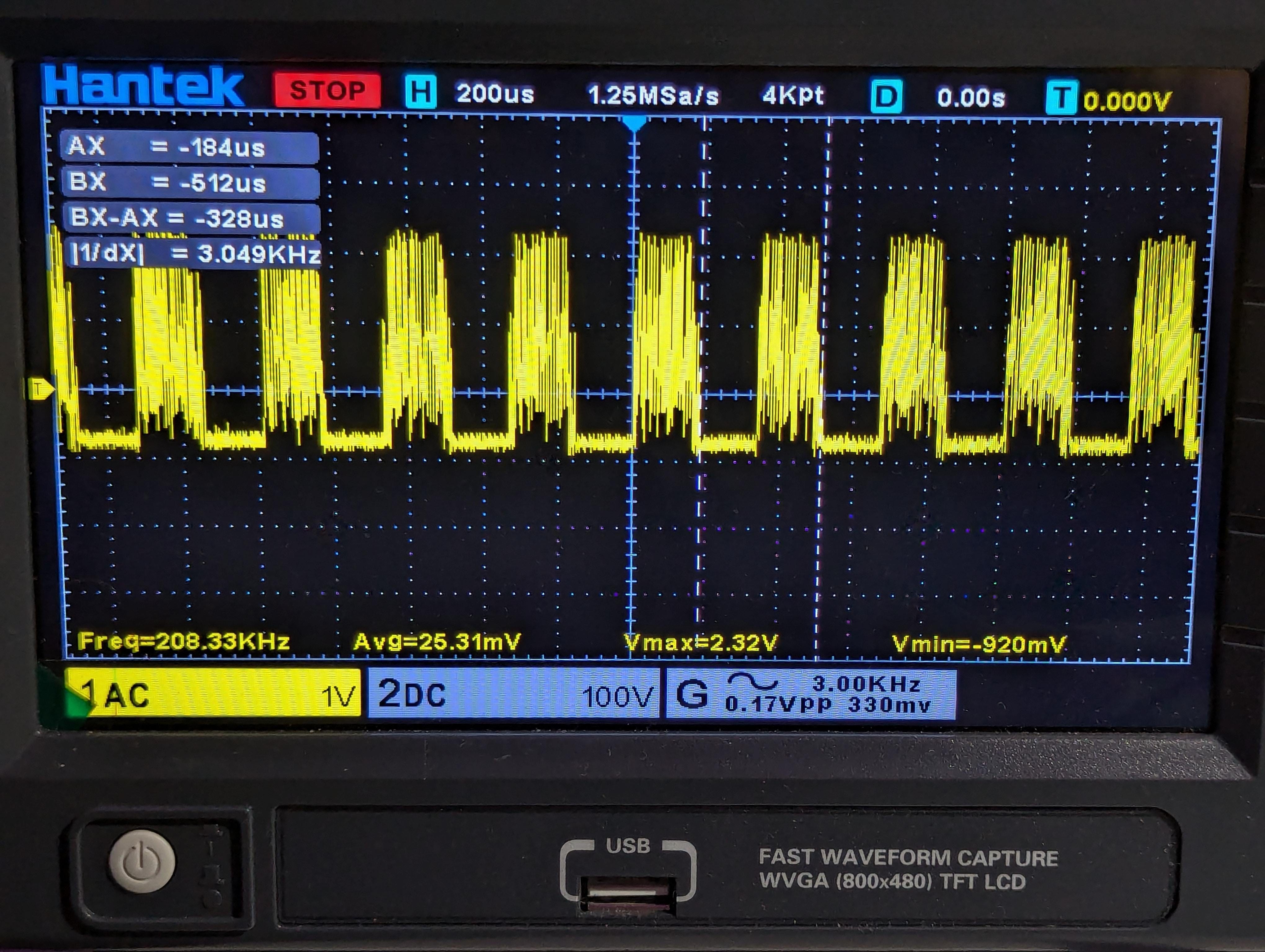
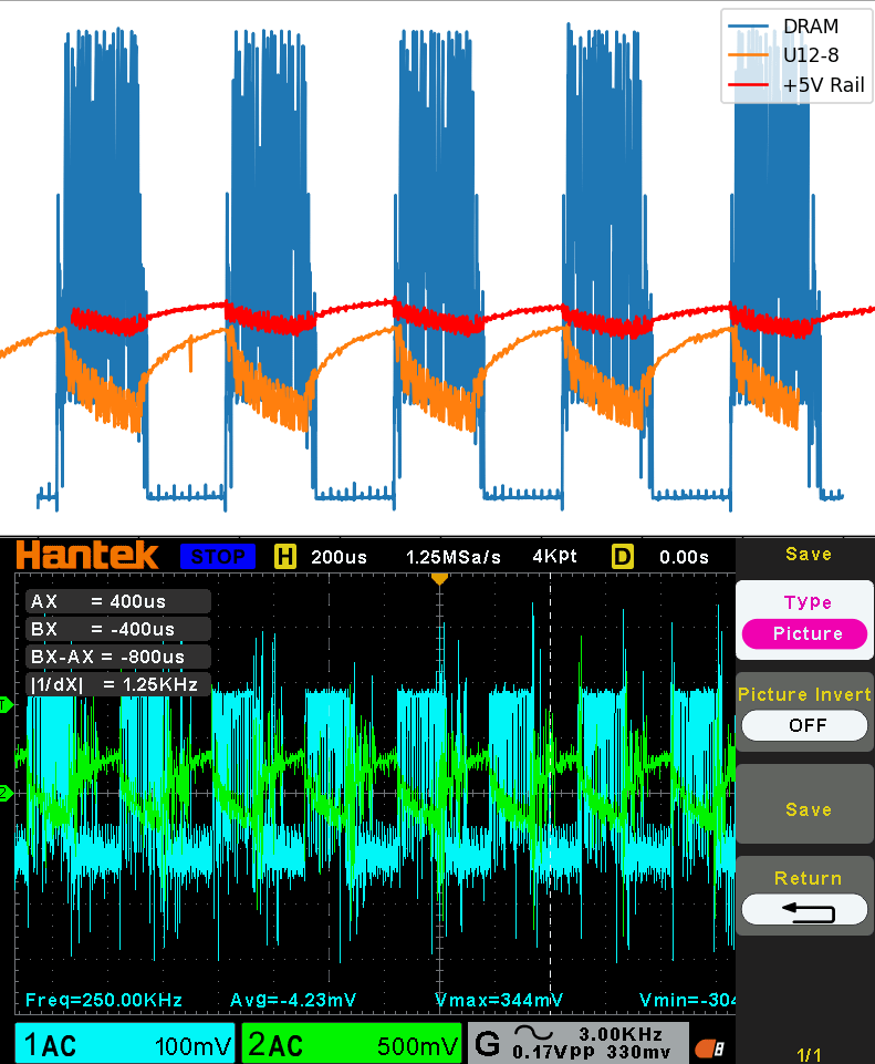
All signs are pointing to noise caused by poor/failing digital power supply rail capacitance that’s coupling into the analog circuits.
Below are all the polymer electrolytic capacitors on the DSP board along with their function. Those in boldface are on digital supply rails.
C1: GUITAR_IN AC coupling capacitor.
C3: +2.5V bulk capacitor (TransTube bias reference - derived from +15V).
C32: Q4 emitter bypass capacitor. Part of TransTube circuit.
C66: +1.2V bulk capacitor. Close to U12.
C72: +28V bulk capacitor. Part of TransTube circuit.
C73: +1.2V bulk capacitor. Near ADSP-21375.
C74: +VD bulk capacitor. Near U3 input.
C75: +3.3V bulk capacitor. Near CS4270.
C77: +1.5V bulk capacitor (TransTube bias reference - derived from +15V).
C78: CS4270 AIN_A AC coupling capacitor.
C79: CS4270 OUTB Sallen-Key filter output AC coupling capacitor.
C80: +15V bulk capacitor. Near Q1/Q2 +5V discrete LDO.
C81: +15V bulk capacitor.
C82: -15V bulk capacitor.
C83: U12 input bulk capacitor.
C84: CS4270 VQ capacitor.
C85: +3.3V bulk capacitor.
C86: +5V bulk capacitor. Near CS4270.
C87: CS4270 FILT+ capacitor.
C88: CS4270 AIN_B AC coupling capacitor.
C91: Q6 emitter bypass capacitor. Part of TransTube circuit.
C99: +3.3VD bulk capacitor.
CMV: Master Volume knob AC coupling capacitor.
SolitaryMassacre tried bolstering the +1.2V and +3.3V rails (both of which are directly associated with the ADSP-21375 and SDRAM, and therefore have the highest ripple) with additional 100uF electrolytics, and there was no perceptible change. The ripple magnitude remained the same and the 3kHz tone was still audible on the audio outputs.
Next, by chance a second DSP board was sourced. Swapping the boards, the same problem was exhibited by the new board. At this point there what we had was essentially a Ship of Theseus; substituting the internal power supplies for bench power, and replacing the DSP board entirely, yet the problem still persisted. This leaves only two options:
This tone is inherent to the design of the DSP board (design flaw)
The boards aren’t assembled ‘correctly’ into the chassis (missing fasteners, etc.) and ‘correct’ assembly results in proper grounding
If it is an assembly problem, this still points to a design flaw likely caused by the convoluted grounding setup in this system (see Grounding section). Fasteners should never be relied for electrical grounding within a board. The board should function the same way (save for any safety earth functionality) irrespective of whether it’s assembled into a chassis or sitting disembowelled on the bench.
If one is concerned about digital and analog return currents interfering within a board, this is almost always better managed through careful and considerate component placement rather than carving up splits in planes and using single point grounds. Rarely is an engineer going to be able to know better than reality itself, the optimal return path for a current, especially across the range of frequencies within the design. With tight component placement that minimises loop areas from signal source to sink, one essentially guarantees that return currents remain local and underneath the components as frequency increases (ref. return current for microstrip/stripline conductors), which will inherently prevent intermingling with other return currents. Plane splits are almost always a bad idea for anything other than galvanically isolated domains.
No posts
Comments
Nothing yet. Say the first thing.
Sign in to join the conversation.