
When we think of glass substrates, we immediately go to the most talked about sectors of chips and advanced packaging. We’ve already heard about vocal demand for glass in chips packaging from Apple, Amazon, Tesla, Intel, Broadcom, and Samsung.
However, I also look at Glass potentially becoming a key building material for three other fast-growing tech areas: next-generation wireless (6G), high-speed fiber optics, and Space.
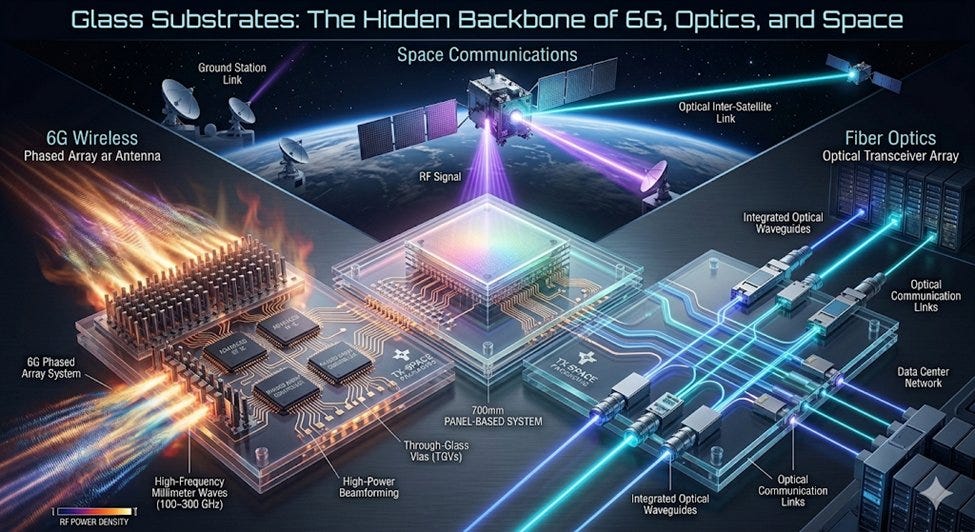
Glass is emerging as a critical material capable of transmitting signals with minimal loss while handling extreme thermal conditions. Let’s break down the three key areas where this matters most, along with a quick look at why Schmid is uniquely positioned to benefit.
Fiber optics is essentially the same story. Keeping latency as low as possible, but instead of radio waves, we’re talking about light.
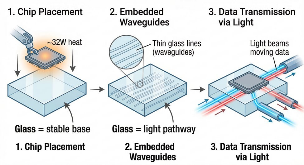
New data centers aim to move data using very little energy (about 5–15 picojoules per bit). For example, a high-speed optical chip can generate around 32 watts of heat in an area the size of a postage stamp.
NVIDIA NVDA 0.00%↑ recently announced optical switches running at 1.6 terabits per second per port, claiming 3.5x energy savings. This is the scale of the problem glass is being asked to solve.
Now, glass plays two roles here. First, as a stable, precise platform for mounting and connecting components. Second, and more interestingly, as the optical “wire” itself, a glass waveguide that guides light the same way a fiber optic cable does but built directly into the substrate.
At a major optics conference (OFC 2025), researchers showed a glass waveguide system that connected six optical transceivers and a shared laser using standard plug-in fiber connectors, with a total signal loss of just 3 dB or less.
The “standard connector” part is the headline, because one of the biggest fears in next-gen data center design is:
What happens when something breaks and you need to replace a component?
Standard connectors mean you can unplug and swap things out, just like a USB cable, instead of having everything permanently fused together.
Corning ($GLW) and GlobalFoundries ($GFS) turned this idea into a product called GlassBridge, a detachable glass waveguide connector aimed at AI data centers that need both high bandwidth and the ability to service and upgrade equipment over time.
In terms of raw performance, glass waveguides can carry light with a loss of just 0.034 dB per centimeter, and they can be manufactured on panels as large as 255 mm x 420 mm, roughly the size of a piece of poster board, which is important for making them economically viable at scale.
6G is pushing wireless signals into much higher frequencies than today’s 5G: Such as 100 to 300 GHz. The reason is simple: higher frequencies carry more data. We’re talking about connections fast enough to transfer a terabyte, roughly 200 Netflix movies, in a single second and supporting 10x more connected devices per square mile than 5G.
But with higher frequencies, signals weaken fast. Imagine trying to shout across a football field, the further you go, the quieter your voice gets.
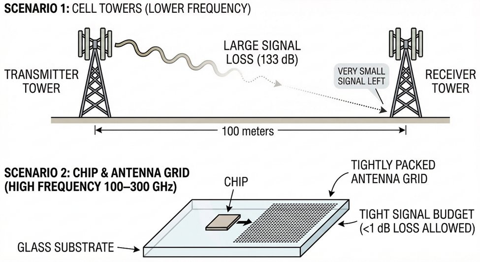
At 140 GHz over just 100 meters, the signal loses so much strength (about 133 dB worth, which is an enormous amount) that the hardware packaging holding everything together can only afford to waste about 1 dB of signal on its own, roughly 1% of the remaining power.
Geometry is the next problem.
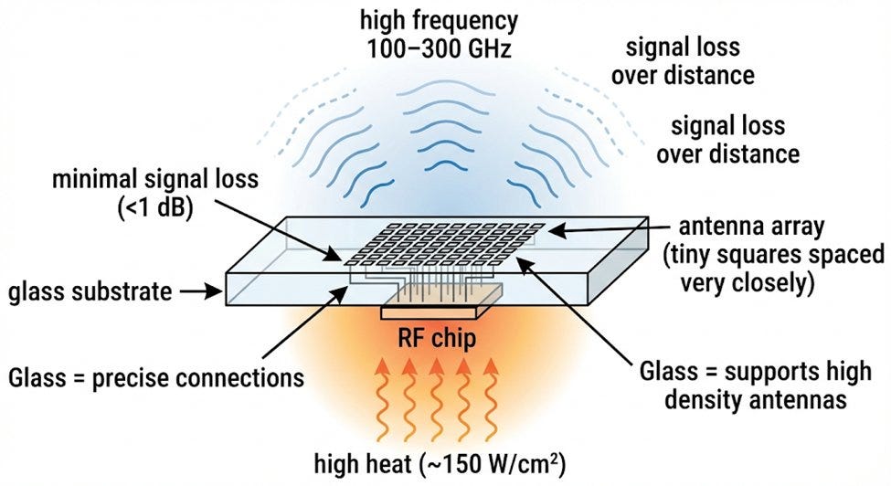
Because these high-frequency signals have very short wavelengths, the antennas that send and receive them must be packed extremely close together, as little as half a millimeter apart at the highest frequencies. That means the circuit board or substrate holding everything needs to be manufactured with extreme precision.
Heat is the third challenge.
These transmitters generate around 150 watts per square cm. That’s like focusing the heat of a hair dryer onto an area smaller than a postage stamp. Glass substrates need to handle this while staying thin (about half a mm to 1 mm thick).
The job of glass in 6G is to hold RF chips right next to their antennas, with precise connections, losing almost no signal, while managing heat.
Space electronics holds the same constraints you see in 6G and fiber optics into a harsher operating envelope:
Extreme reliability expectations, thermal cycling, and long service lifetimes while still needing high‑bandwidth RF and optical links.
SCHMID itself explicitly calls out renewed investment in “aerospace electronics” as part of a healthier order pipeline in Europe and North America, which is a useful clue that the company (and its customers) view aerospace as a real end market for next‑gen substrate tech.
On the “what would it be used for?” side, SpaceX’s own published Starlink technical overview helps frame the payload mix: Starlink satellites use multiple Ku‑band phased‑array antennas plus Ka‑band and E‑band antennas, and they also include optical inter‑satellite links (“space lasers”) operating up to 200 Gbps.

In practice, “glass substrates in space” would show up as rigid, ultra‑flat panels or modules that carry dense RF routing and antenna structures (electrical role), and/or as glass panels that incorporate optical routing features and connector interfaces (optical role).
The key idea is the same as on Earth: keep loss low and geometry precisely because arrays (RF) and connectors/couplers (optics) punish slop.
A good way to visualize the electrical case is beamforming/RF chips mounted very close to the antenna array, with vertical and lateral interconnect built into the substrate to minimize distance and discontinuities.
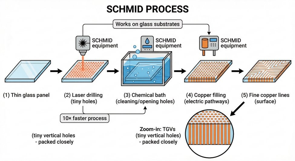
The simplest way to understand what SCHMID does is to think about what it takes to manufacture glass substrates at scale.
You need to: (1) drill millions of tiny holes through thin glass, (2) clean those holes precisely, (3) fill them with copper so electricity can pass through, (4) create extremely fine circuit traces on the surface, and (5) do all of this on large panels, fast enough to be worthwhile. SCHMID makes the equipment that handles every one of these steps.
The “holes in glass” problem is harder than it sounds. SCHMID works with TRUMPF (a major laser company) to develop a process where a laser first modifies the glass structure, and then a chemical bath etches out the holes.
The result is a claimed 10x speed improvement over older methods.
This matters because a single antenna array package might require millions of these tiny vertical connections, called through-glass vias, or TGVs, and you can’t afford for each one to take forever.
SCHMID’s own recent 20F filings describe a process called Embedded Trace (ET), which uses plasma (a superheated, electrically charged gas) rather than traditional laser drilling to create circuit traces. It embeds those traces in insulating material and fills them with copper in a proprietary process.
The company’s own documents state that this ET process is compatible with glass cores, meaning it can work directly on the glass substrates that both 6G and fiber optics need.
Rather than just supplying one piece of equipment, SCHMID positions its glass workflow as end-to-end: starting with via formation and copper plating, through building out the redistribution layers (the fine surface wiring that connects everything).
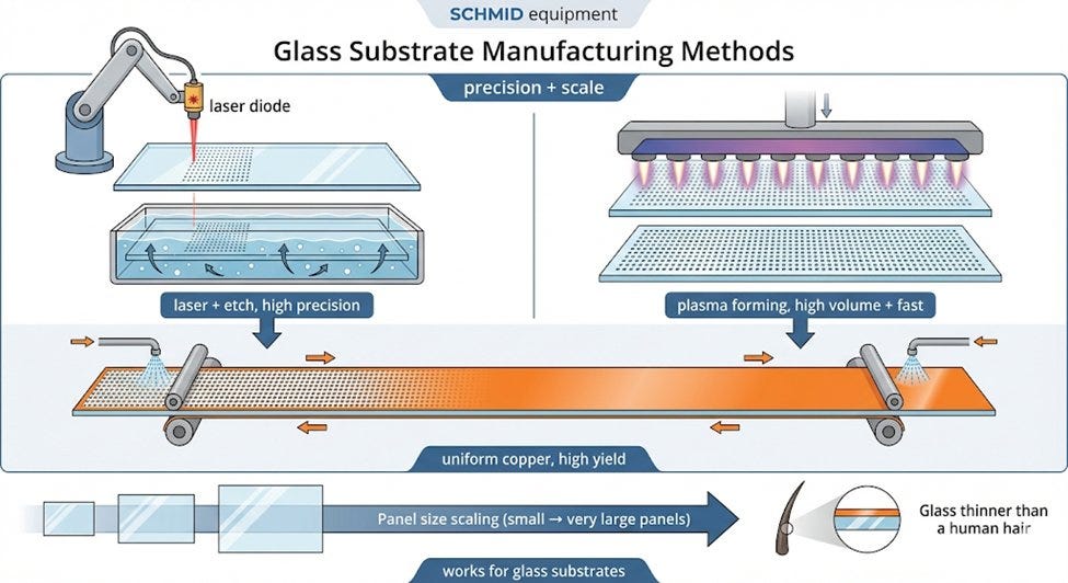
Its HPPF process, High Performance Plasma Forming, is designed to replace laser drilling for certain via types, which is important when you’re trying to make millions of holes quickly and consistently.
These etching systems can handle panels ranging from 100 mm x 100 mm all the way up to 600 mm x 600 mm. This size flexibility matters because the economics of glass substrates depend on being able to process large sheets efficiently.
One key challenge is making sure copper spreads evenly across the whole panel, not thicker in some spots and thinner in others. SCHMID’s system is built to control this and keep it uniform. If the copper isn’t even, production doesn’t work on a scale.
Even the plasma cleaning steps matter. SCHMID’s PlasmaLine system handles simultaneous double-sided processing and includes both etching and metal deposition for adhesion layers, the thin glue-like layers that make copper stick to glass. It handles panels from 12”x 18” up to 24”x 24” and substrates as thin as 10 micrometers (roughly one-tenth the thickness of a human hair).
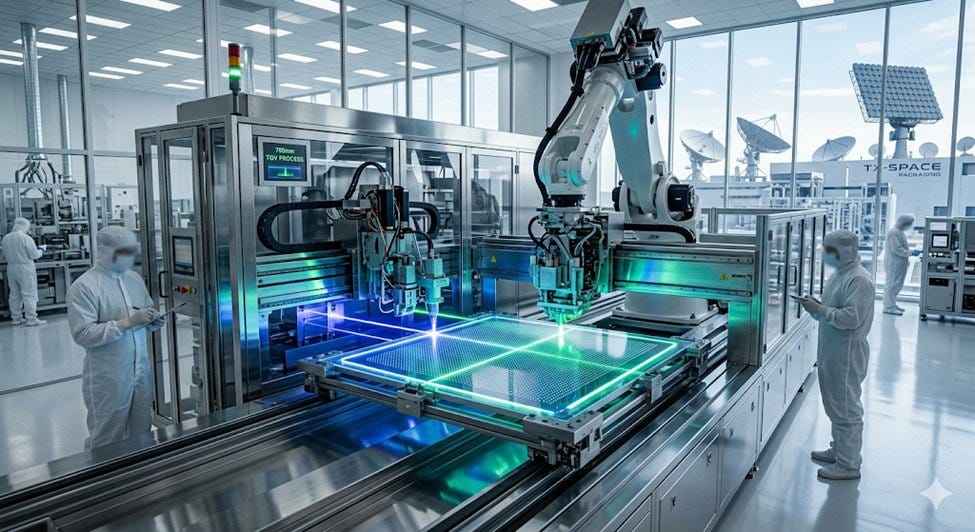
The “scale” datapoint that keeps comes up in public reporting is panel size. Tom’s Hardware reported that SpaceX is (reportedly) expanding into fan‑out panel‑level packaging and aiming for a packaging facility in Texas, citing an unusually large 700 mm x 700 mm substrate format.
Separately, San Antonio Express-News reported SpaceX is investing to expand semiconductor research/manufacturing in Bastrop County tied to its Starlink factory footprint, including circuit board production and advanced packaging technologies.
SCHMID’s tooling roadmap aligns well with large-scale aerospace manufacturing, focusing on panel-level processing, high cleanliness, and repeatability—key for producing consistent RF/optical modules. Its capabilities include TGV etching (100×100 mm to 600×600 mm) and advanced plating and surface prep for glass-based substrates.
SCHMID also delivered an InfinityLine H+ system (up to 700×700 mm panels) to an unnamed U.S. tech company. While some link this to SpaceX due to similar scale interests, there is no confirmed relationship, and it was only one machine per their PR.
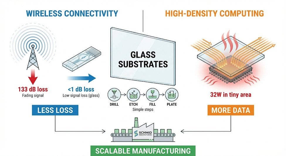
Here’s the deal worth remembering: These application are trying to solve the same fundamental problem: moving more data with less loss and less wasted energy, at scales that are getting harder and harder to achieve with traditional materials. Glass substrates are emerging as the answer in both cases, just in different forms: electrically for wireless, and optically for fiber optics.
The physics are unforgiving. In wireless, you’re working against a 133 dB signal loss over 100 meters with only 1 dB to spare in your hardware. In optics, you’re trying to fit 32 watts into a postage stamp while keeping every connection loss under control. In space, you’re dealing with extreme temperature swings and radiation while still needing precise, low-loss performance. In both cases, the manufacturing process = drilling, etching, filling, plating, and connecting glass at scale. That is what determines whether glass stays a lab curiosity or becomes the possible backbone of industries.
SCHMID’s relevance comes from its end-to-end tooling for manufacturing glass substrates at scale, covering every critical step from via creation to plating and surface processing. Its documented processes include laser-plus-etch TGV formation, plasma-based Embedded Trace technology compatible with glass cores, and panel-scale plating systems designed to ensure copper uniformity for high-volume production.
I see these areas being largely overlooked and underappreciated in the broader glass substrate narrative.
No posts
Comments
Nothing yet. Say the first thing.
Sign in to join the conversation.