
For busy people — five things this post claims:
Huawei just proposed replacing Moore’s Law. Its “Tau Law” folds chips vertically instead of shrinking them — claiming TSMC-class density without a single ASML machine. The claim gets tested by an electron microscope in six months. We know the date.
The uncomfortable secret: the whole industry is going vertical anyway. TSMC, Intel, Samsung, and IBM are racing to the same stacked-transistor destination (CFET) — arriving in 2031, the exact year of Huawei’s promise. China isn’t leaving the road. It’s sprinting the consensus route without a ticket.
The quiet winner may be Japan. It lost the war of printing chips forty years ago — but it already owns the tools of stacking them (Disco, Advantest, Tokyo Electron). Japan sits where ASML sat in 1995: the boring supplier of a transition nobody has priced yet.
One layer up, the movie already ended — and we can watch the finale. The price of intelligence fell ~1,000× in three years. Days ago, China’s Kimi K3 — the largest open-source model in history — started charging frontier prices. That’s what the endgame looks like when the alternative becomes credible.
Tokens are becoming crude oil. Quality grades, a forward market, demand shocks, a cartel tighter than OPEC, and a national-security file. The durable margin migrates to the “refineries” — ontologies. Don’t own the well. Own the refinery.
If you only read one section, read VIII. If you read two, add IX — the case against everything above.
In January 2025, DeepSeek proved that restriction can be a design algorithm.
Cut off from Nvidia’s best chips, a Chinese lab trained a frontier model for a fraction of the cost. It didn’t compete on the same curve. It changed the curve.
Sixteen months later, on May 25, 2026, He Tingbo — president of HiSilicon, China’s “queen of chips” — walked onto the IEEE ISCAS stage in Shanghai and proposed doing the same thing to the most famous law in technology.
She didn’t announce a machine. She announced a law.
She called it the Tau Law (τ). Her peers already call it He’s Law.
Moore’s Law was never a law of physics. It was the exponential phase of an S-curve that lasted sixty years.
The logic was simple: shrink the transistor and everything improves. More density, more speed, less energy. One axis of progress: the horizontal. Smaller features, printed with ever more extreme lithography.
But every S-curve matures. And this curve’s maturity has a name and an address: Veldhoven, Netherlands. A single company — ASML — builds the only EUV machines on the planet. Each High-NA machine costs ~$400 million. Each generation costs more, yields less, and is available to fewer players.
When an entire industry’s progress concentrates in a single supplier, you are not in the exponential phase. You are in saturation.
And in the saturation of one curve, the next one is born.
Huawei’s proposal is a change of variable.
Moore optimizes space: transistors per square millimeter, achieved by shrinking geometry.
Tau optimizes time: the signal propagation delay (τ), compressed at every level of the architecture.
The practical implementation is called LogicFolding: instead of shrinking circuits within the 2D plane of the wafer — which requires EUV — it folds them vertically into stacked floors. Skyscrapers of logic instead of denser suburbs.
The numbers Huawei publishes for the Kirin 2026, the first commercial chip with this architecture:
+53.5% transistor density: 238 million per mm², theoretically at the level of TSMC’s N3 and Intel’s 18A — without EUV.
−41% power consumption at equal performance versus the Kirin 9030 Pro.
−30% wire length, −50% clock buffers, −25% clock skew.
In He Tingbo’s words: the gains came “not through a new lithographic step, but through a topological reorganization of the spatial distribution of logic.”
Translation: design as a substitute for the machine.
It is exactly the DeepSeek pattern. When they block your hardware, you turn architecture into your lithography.
And the math is elegant. Signal delay grows with the square of distance (τ ∝ L²). Cut wiring by 30% and you gain 51% in time. A linear cut buys a quadratic gain. That is where the entire trick lives.
Here is the fact almost nobody connects.
Vertically stacking logic is not a Chinese invention. It is the consensus destination of the entire industry. It’s called CFET — Complementary FET — and it stacks NMOS and PMOS transistors on top of each other instead of side by side.
TSMC demonstrated the first functional CFET circuit at IEDM 2025: a 101-stage ring oscillator and the world’s smallest SRAM cell, with gate pitch below 48nm.
Intel was first to demonstrate CFET (2020) and already integrates it with PowerVia, its backside power delivery.
Samsung achieved the industry’s smallest 3D-stacked transistor in June 2026: 42nm gate pitch. Best Paper at VLSI.
Imec, the industry’s oracle, places CFET’s commercial insertion at the A7 node, around 2031.
Read that date again. 2031. The same year Huawei promises 1.4nm-equivalent density.
Two parallel S-curves, same direction, same deadline. The difference is not the what. It’s the why:
The West stacks WITH EUV lithography — vertical scaling as the next step after horizontal.
China stacks INSTEAD OF EUV lithography — vertical scaling as the substitute for the horizontal path it was denied.
One is evolution. The other is mutation under selective pressure.
And evolutionary biology is clear about what pressure produces: acceleration.
The vertical transition is not one company — it is the entire ecosystem reorganizing in five layers. Stacked transistors at the bottom (TSMC, Intel, Samsung, and IBM’s new sub-1nm “nanostack”). Backside power delivery above it (Intel’s PowerVia shipping now; TSMC’s version arrives with A16 this year). Die stacking where the third dimension is already a business, not a promise (AMD’s 3D V-Cache since 2022; TSMC’s ~$18 billion packaging franchise). A state-backed newcomer (Rapidus — next section). And the toolmakers who sell shovels to everyone. Advanced packaging grows from ~40% of its market in 2020 to a projected 60%+ by 2030.
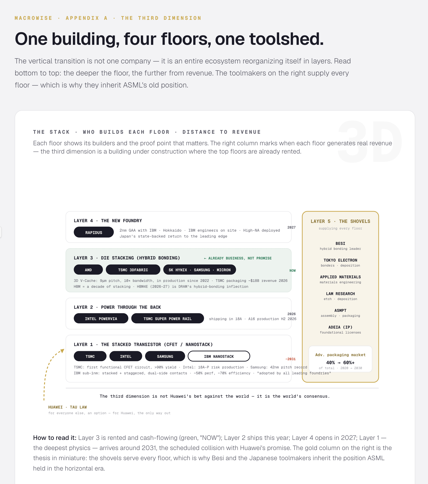
One sentence carries the whole section: the third dimension is not Huawei’s bet against the world — it is the world’s consensus, and Huawei is simply the only player for whom it isn’t an option but the only way out.
There is a third player in this transition that almost nobody is reading correctly.
Japan lost the horizontal war. In the eighties it dominated global DRAM; Korea and Taiwan took fabrication away, and for thirty years Japan looked like a semiconductor museum. But look at what the vertical era demands — stacking, thinning, bonding, testing — and you find a pattern uncomfortable for everyone else: the tools of stacking are already Japanese.
Disco holds a near-monopoly in grinding and dicing — thinning wafers to tens of microns, the physical prerequisite of all stacking. You cannot build silicon skyscrapers without Disco’s foundations.
Tokyo Electron builds the bonders and deposition systems of the 3D chain; Advantest dominates test — and testing stacked dies (where one defective floor kills the whole tower) is the central economic problem of 3D.
Shin-Etsu and SUMCO control the silicon wafer; JSR and TOK, the photoresists. Materials and precision mechanics: exactly Japan’s industrial DNA.
Kioxia was the world’s pioneer of hybrid bonding in production: NAND bonded with the technique since 2023, before anyone in logic.
And on top of that tool base, the frontal bet: Rapidus. Backed by the Japanese state, its IIM-1 line in Hokkaido already runs the 2nm GAA process developed with IBM — IBM engineers on site, ASML High-NA EUV deployed, mass production toward 2027. And since its roadmap is IBM’s roadmap, sub-1nm nanostack is the next technology down that pipeline.
The strategic read: Japan lost the war of printing. The vertical era is played in cutting, polishing, bonding, and testing — the four things Japan never stopped dominating. While the U.S. and China fight over lithography, Japan already owns the shovels of the next gold rush. Japan occupies the exact position ASML held in 1995: the boring supplier of a transition nobody valued yet.
If LogicFolding bends the current curve, carbon nanotubes skip the curve entirely.
2017. Peng Lianmao’s team at Peking University publishes in Science: carbon nanotube (CNT) transistors that outperform silicon at the same scale.
2024. The same center publishes in Nature Electronics a carbon nanotube TPU: 3,000 CNT transistors running convolutions and matrix multiplication. A 5-layer neural network hits 88% accuracy on MNIST consuming 295 microwatts. Not a lab transistor — a functional AI accelerator in a post-silicon material.
March 2025. Beijing presents the first carbon AI chip with ternary logic — three states instead of 0 and 1. More information per signal, less energy per computation.
September 2025. The key report: Huawei is preparing with SMIC a “3nm carbon-based” design — carbon nanotubes and 2D materials on GAA architecture. Lab validation complete; adaptation to SMIC production lines underway, design tape-out targeted for 2026.
Why it matters: CNTs have a strategic property silicon doesn’t. They don’t need EUV to compete. Their advantage comes from the material, not the geometry. It is the third S-curve — the most immature, the most speculative, and the only one that would make the entire sanctions infrastructure irrelevant.
The complete chain China is assembling: material physics (Peking U.) → architecture (Huawei LogicFolding) → fabrication (SMIC + SMEE lithography) → domestic EDA. In He Tingbo’s words: “I thought it would take ten years; we got here in six.”
Everything above happens in the silicon layer. But the same pattern has already played out — complete, measurable, with prices — one layer up: in the cost of intelligence itself.
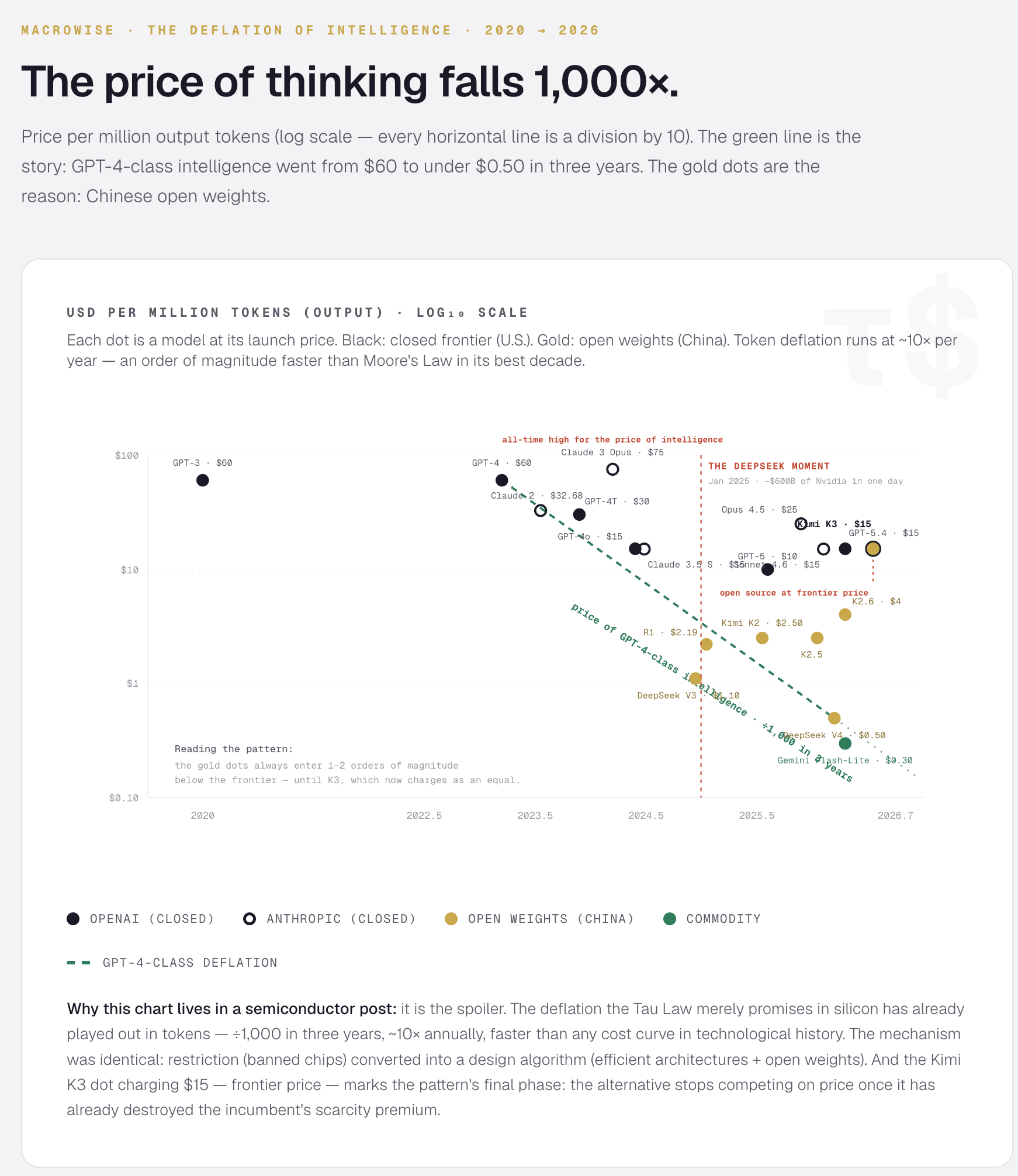
The numbers of the collapse: a million tokens of GPT-4 cost $30–60 in March 2023. Today, intelligence of that same class costs under $0.50 per million — a ~95% drop in two years and close to 1,000× in three. a16z called it “LLMflation”: 10× annual deflation, sustained, and accelerating.
The Kimi case is the most instructive, because it shows the pattern twice:
Moonshot AI nearly died from DeepSeek. After January 2025’s R1, Kimi fell from third to seventh place in Chinese users. Its response was to become the thing that almost killed it. It pivoted to open source with Kimi K2: July 2025, one trillion parameters, #1 in Hugging Face downloads on launch day. The community called it “another DeepSeek moment.”
Since then, the cadence: K2.5 (January 2026) with swarms of 100 parallel agents at 76% lower cost than Anthropic’s premium model. K2.6 (April) tying GPT-5.5 on the coding benchmark that matters, 80% cheaper, weights downloadable. And days ago, Kimi K3: 2.8 trillion parameters, the largest open-source model in history, shoulder to shoulder with proprietary frontier systems. Moonshot went from near-irrelevant to a ~$20 billion valuation in eighteen months.
Note the pricing detail nobody comments on: K3 charges $3/$15 per million — frontier price. Chinese open source is no longer the cheap tier; it is the alternative tier.
Here is where the two halves of this post fuse into one market structure. Because if you look at what tokens are becoming, you are not looking at software pricing. You are looking at the birth of a commodity market — and the closest historical template is oil.
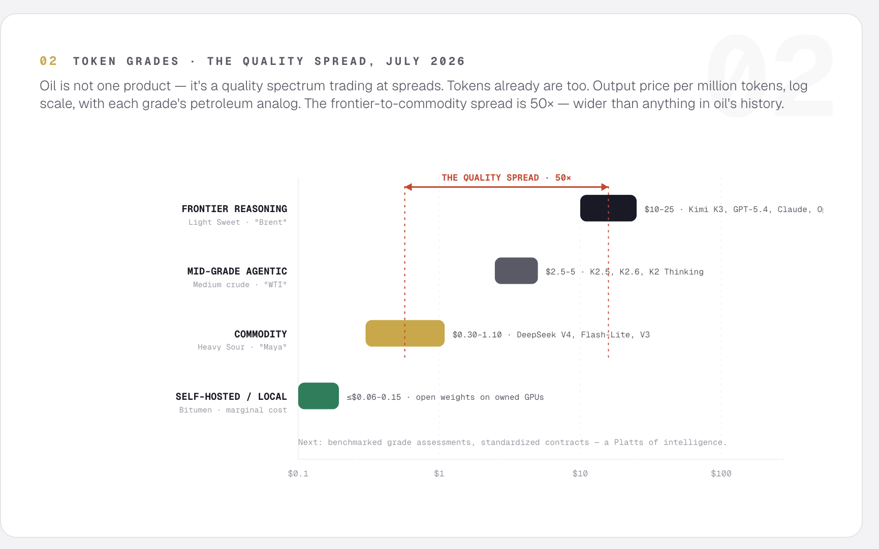
Grades and spreads. Oil is not one product; it’s a quality spectrum — Brent, WTI, Maya — trading at spreads. Tokens already are too: frontier reasoning tokens (Kimi K3, GPT-5.4, Claude at $15/M output) are the light sweet crude; commodity tokens (Flash-Lite at $0.30) are heavy sour. That’s a 50× quality spread, wider than anything in petroleum, and it will be quoted — benchmarked grades, standardized contracts, a Platts of intelligence publishing daily assessments per capability class.
Futures and the financialization of compute. The forward market already exists in embryonic form: CoreWeave’s take-or-pay contracts, hyperscaler capacity commitments, Nvidia allocation agreements — these are forward contracts on compute, just bilateral and illiquid. The next step is obvious to anyone who has watched a commodity market mature: standardization → clearing → futures curves → speculation → volatility term structure. When you can trade March-2028 delivery of a petaflop-hour, compute has become oil. And the token is its refined retail product — the gasoline at the pump.
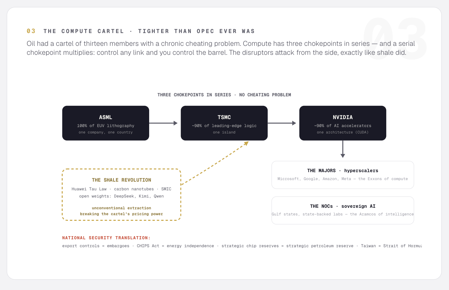
Demand shocks and the volatility everyone underestimates. Oil’s history is demand surprising supply — and tokens have a built-in demand accelerant oil never had: reasoning models consume up to 100× more tokens internally than they output. Agent swarms multiply this again. This is why token prices fall 80% while enterprise AI bills double — a paradox any oil economist recognizes instantly as Jevons. Falling prices don’t shrink the market; they detonate it. Expect demand-driven price spikes, capacity crunches, and the token equivalent of the 1973 gas line: inference queues during compute shortages.
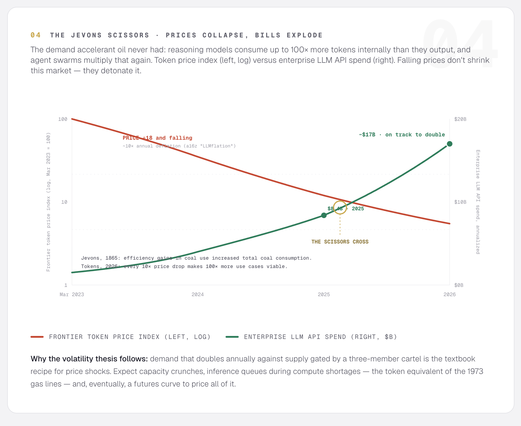
The cartel. Oil had OPEC. Compute has something tighter: the ASML–TSMC–Nvidia chokepoint is a de facto supply cartel with three members and no cheating problem. Hyperscalers are the majors; sovereign AI programs (the Gulf states, China’s state-backed labs) are the national oil companies. Export controls are embargo politics under a new name. This is why the entire post above is, at bottom, a national security document: chips are already treated exactly like oil was in the twentieth century — strategic reserves (the CHIPS Act is energy independence policy), sanctions as embargoes, and Huawei’s Tau Law as the shale revolution: the excluded producer inventing an unconventional extraction method that breaks the cartel’s pricing power.
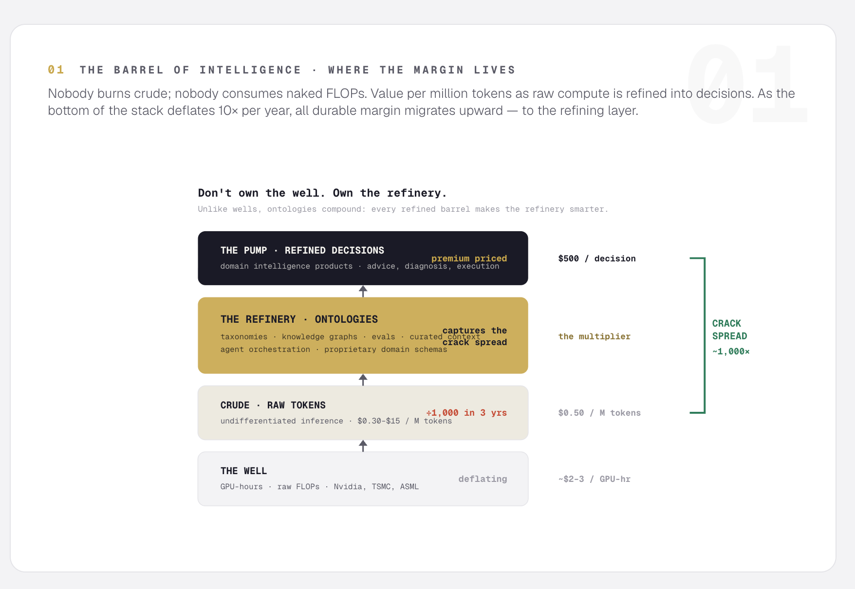
And the piece everyone is missing: crude is useless without refineries. Raw compute — like raw crude — has almost no end-use value. Nobody burns crude; nobody consumes naked FLOPs. Between the well and the pump sits the refinery, and the refinery captures the crack spread. In the intelligence economy, the refineries are ontologies. The structured knowledge layer that turns undifferentiated tokens into reliable, domain-specific intelligence: taxonomies, knowledge graphs, evaluation frameworks, curated context, agent orchestration, proprietary data schemas. The semantic infrastructure that converts $0.50 of raw tokens into $500 of decision. As raw token prices collapse toward zero, all the margin migrates to the refining layer. The well owners fight deflation; the refiners capture the spread between commodity input and refined output.
The investment translation: in the 1,000× token deflation, don’t own the well. Own the refinery. Whoever builds the dominant ontologies of finance, medicine, law, and logistics becomes the ExxonMobil downstream of the intelligence economy — and unlike wells, ontologies compound: every refined barrel makes the refinery smarter.
Where the analogy breaks — and why the break matters more. Honesty requires the disanalogies: oil is scarce and burned once; tokens are manufactured and infinitely replicable. Oil moves in tankers; tokens move at lightspeed for free. Oil demand is inelastic — you drive to work regardless of price; token demand is hyperelastic — every price drop invents new demand. But notice what each break implies. No scarcity means the deflation is permanent, not cyclical: there is no depletion to rescue the well owners. No transport cost means no geographic pricing power — no Rotterdam premium, no Henry Hub. And hyperelastic demand means the volatility comes from the demand side, not supply — the opposite of oil’s structure, and harder to hedge. The analogy’s failures don’t weaken the thesis. They radicalize it: tokens are oil with the well owners’ every historical advantage removed.
The strategic synthesis of the whole post: China’s strategy is coherent across every layer of the tower. At the top, open weights commoditize the model — destroying OpenAI’s and Anthropic’s scarcity rent. At the bottom, Tau and carbon attack ASML’s and TSMC’s scarcity premium. Commoditize the complement you don’t control. And in both layers, the mechanism is identical: restriction (banned chips above, banned EUV below) converted into a design algorithm. Token deflation is the spoiler for the silicon movie: this is what the ending looks like when the alternative becomes credible.
Every honest thesis needs its devil’s advocate. The other side of the book:
1. No figure is verified. All numbers are Huawei’s, against its own baseline (Kirin 9030 Pro), not against real TSMC N3 silicon. No independent teardown, no production data, no third-party benchmarks.
2. SMIC remains stuck at 7nm. Paul Triolo (DGA Group): a stacked design yields effective density gains, “but it doesn’t mean Huawei has solved the process, yield, power, thermal, and performance problems associated with actually manufacturing at 1.4nm-class.”
3. Thermal physics doesn’t negotiate. Bernstein warns: stacking logic and memory concentrates thermal density. Transistor skyscrapers are vertical ovens. Stacked silicon heats from the inside.
4. The “1.4nm equivalence” is accounting, not physics. Density is measured by footprint projection: you multiply floors, you don’t shrink pitch. Huawei has form on generous labeling — the Kirin X90 is marketed as “5nm” and is a 7nm design with advanced packaging.
5. ASML isn’t standing still. While Huawei presented slides, ASML pushed EUV throughput to 230 wafers/hour and confirmed the first High-NA products ship within months. The old curve still has slope.
6. The market’s sarcasm. One analyst summarized it without anesthesia: “I have as much confidence in He Tingbo’s 1.4nm chips as in Elon Musk’s Mars colony.”
A thesis that cannot be tested is not a thesis — it’s a religion. So: here is the thesis, here is when reality votes, and here is how to position for either verdict.
DeepSeek didn’t destroy Nvidia. It destroyed the certainty about Nvidia. On January 27, 2025, the market erased ~$600 billion of capitalization in one day — not because DeepSeek was better, but because it proved another path existed.
Huawei’s announcement is the same operation against the certainty of ASML.
Every dollar of Western AI capex implicitly assumes EUV and ASML are the only road to competitive silicon. An alternative supply chain doesn’t need to be better. It needs to be cheaper per unit of useful compute, available, and beyond the reach of future sanctions.
Compute. ASML’s monopoly stops being an axiom and becomes a probability — very high at 5 years, debatable at 10. Monopolies don’t die when the competitor appears; they die when the marginal customer believes an alternative exists. ASML’s valuation premium is a premium of inevitability. Tau is a direct attack on that premium, not on its revenues.
The temporal monopoly, logic edition. Memory already lives in the third dimension: HBM is stacking. Logic is heading to the same place. Competitive advantage migrates from who prints finest to who stacks best — a game of packaging, materials, and design where incumbents hold five years of advantage, not sixty. And the tool layer of that game is disproportionately Japanese and Dutch: Disco, Advantest, TEL, Besi — the refinery equipment makers of the silicon barrel.
Electricity. −41% power at equal performance, if real, is the announcement’s most important number. The bottleneck of the fourth S-curve isn’t silicon — it’s electrons. The winning architecture will deliver more compute per watt, not per nanometer.
The refining layer. As tokens commoditize like crude, the durable margin sits in ontologies — the semantic refineries. In portfolio terms: the well (raw compute) deflates; the pipeline (networking, packaging) earns tolls; the refinery (ontologies, agents, domain intelligence) captures the crack spread. Position accordingly.
And the calendar where all of it gets tested:
Winter 2026 (next 6 months). The Kirin 2026 reaches real phones. The TechInsights teardown is verification event number one: real density measured under electron microscope, not in a keynote. Sustained benchmarks under thermal load — stacking betrays itself in throttling.
2026–2027. Does Huawei’s carbon-based design actually enter SMIC’s lines? Reportable yield or silence?
2027–2028. SMIC yields at 5nm-class with DUV multi-patterning. Cost per transistor is the judge that accepts no propaganda.
2031. The scheduled collision: commercial CFET from TSMC/Intel/Samsung versus Huawei’s 1.4nm-equivalent promise. Same year, two technological civilizations, two routes to the same density.
In 1965, Gordon Moore wrote a four-page article and an industry turned it into destiny for sixty years.
In 2026, an engineer in Shanghai proposed replacing it — not because she found a better idea, but because she was denied the machine that executed the previous one.
The sanctions designed to freeze China on the old curve may end up being the subsidy that financed the new one. Restriction as design algorithm. Again.
In 2025, DeepSeek cost the market $600 billion in a single day. The Kirin teardown arrives in six months. This time, we know the date.
The silicon folds. The question is whether history does too.
Thanks for reading ,
Guillermo Valencia A
No posts
Comments
Nothing yet. Say the first thing.
Sign in to join the conversation.