A USB wiring schematic is only useful when it shows connector role, VBUS handling, D plus and D minus routing, shield grounding, and the CC or ID details that affect a real PCB.
Thermal impedance is only useful when you know whether the datasheet number describes a package test board, a case path, a board path, or a short pulse event in your real design.
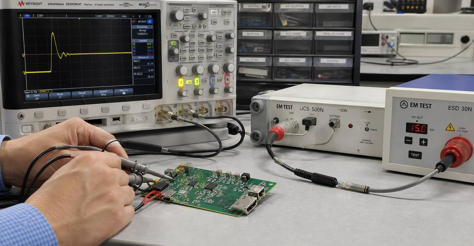
A TVS suppressor diode only protects a PCB when standoff voltage, clamp behavior, surge energy, and layout placement match the actual threat at the connector.
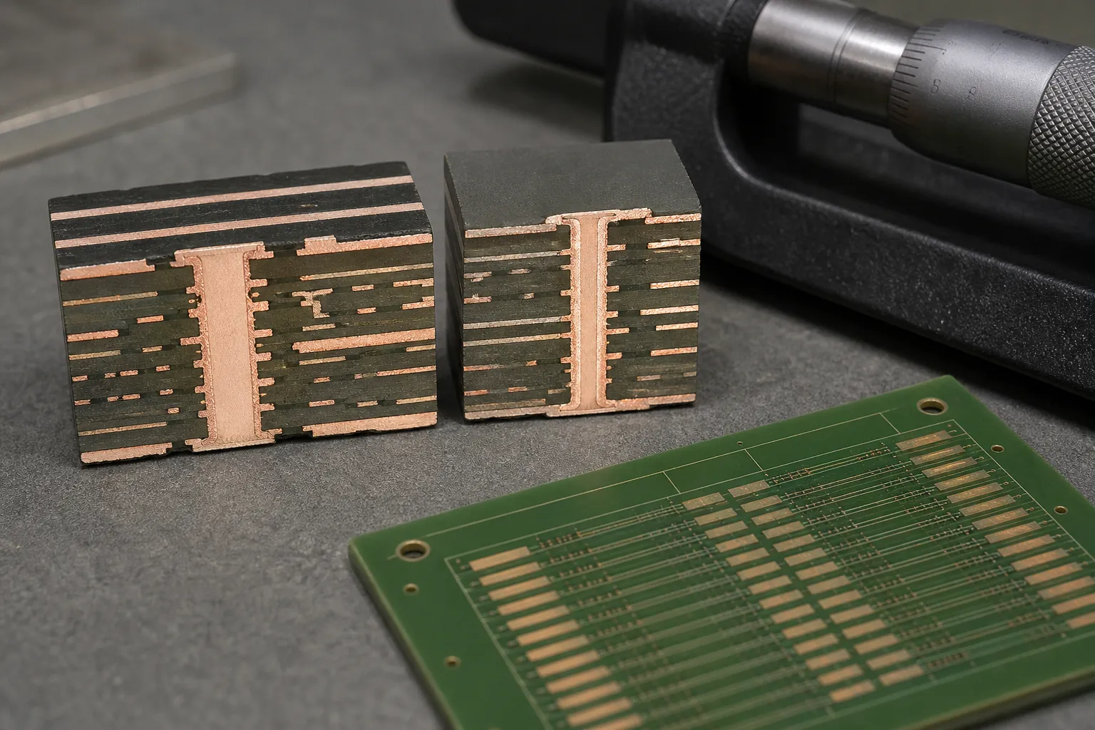
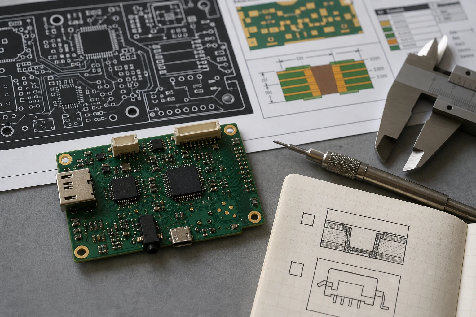
Standard 2-, 4-, 6-, and 8-layer PCB stackups only work when return paths, impedance, copper balance, and fabrication assumptions still match the real design.
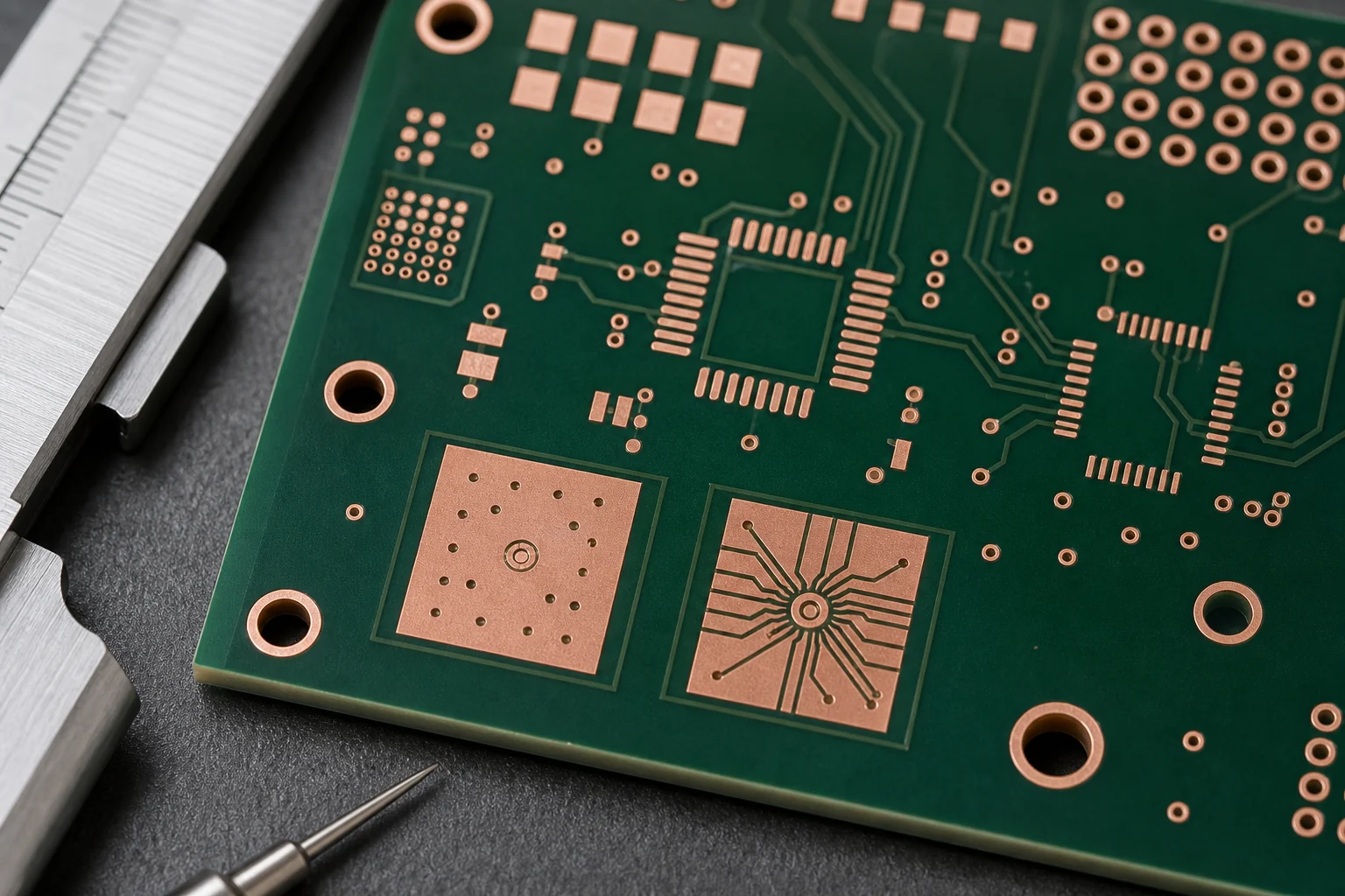
Via in pad can solve dense BGA and QFN escape problems, but only when fill, cap, planarity, paste behavior, and inspection risk are reviewed before release.
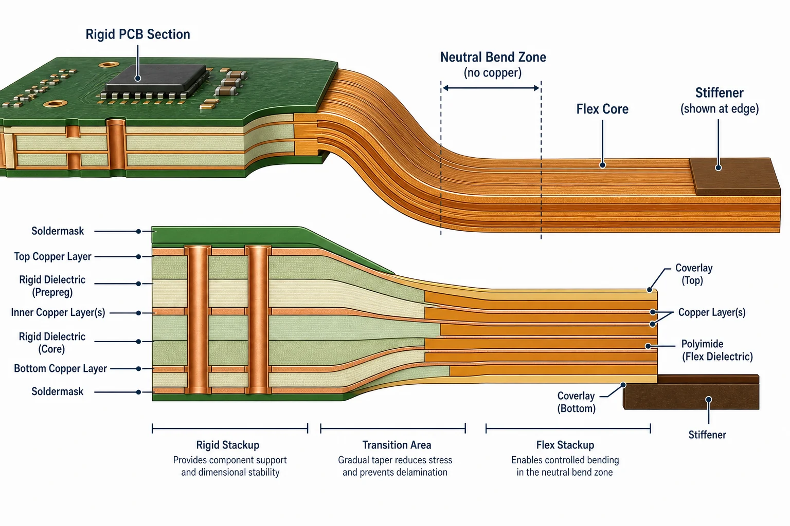
A rigid-flex PCB stackup is not just a layer list. It sets bend reliability, copper strain, stiffener transitions, impedance behavior, and assembly risk long before fabrication starts.
If you want to create a KiCad design from text, start with structured parts, named nets, power assumptions, and ERC checks so the generated schematic stays editable and reviewable.
Moving a legacy Protel design into Altium Designer is not just a file-open task. This guide covers libraries, rules, polygons, outputs, and verification steps that keep old boards manufacturable after migration.
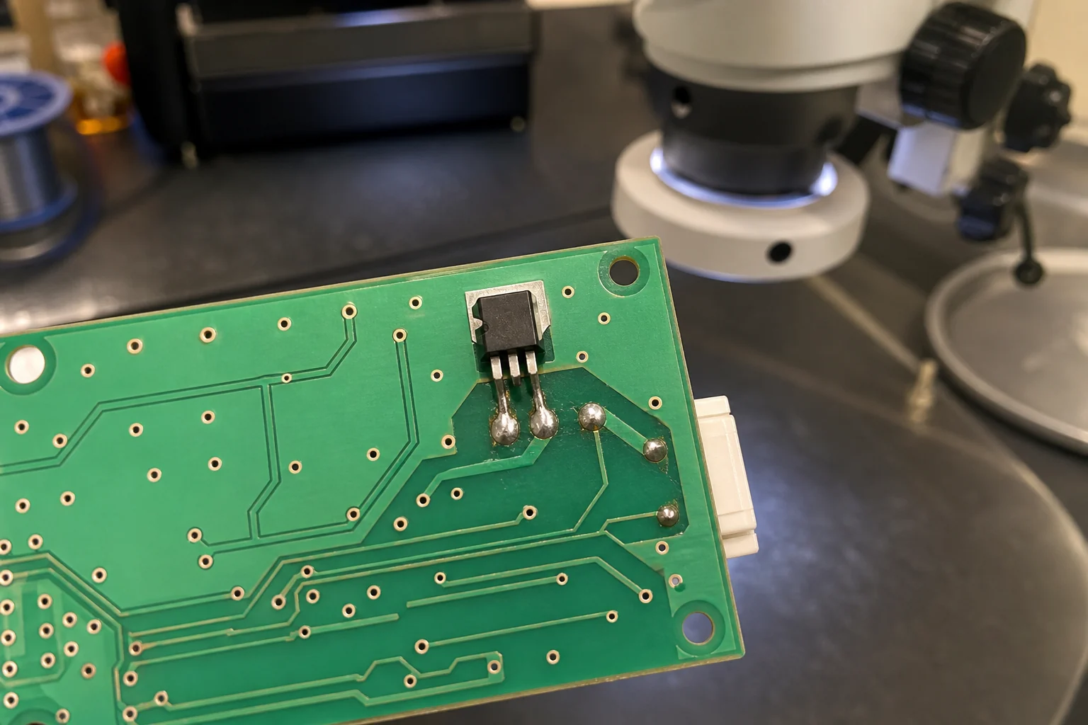
Choosing the smallest N-channel MOSFET through hole package means balancing gate drive, fault energy, thermal margin, pinout, and rework access on the real PCB.