
For most of the AI boom, the semiconductor investment map was fairly easy to understand. Nvidia and the custom-chip designers created the architectures. TSMC manufactured them. The memory companies supplied HBM, while the packaging companies assembled the pieces into a finished accelerator.
Testing sat somewhere near the end of that map. It was important, of course, but I initially thought of it as a supporting business: more chips would be produced, more chips would need to be tested, and the equipment suppliers would benefit from the additional volume.
The latest earnings season made that explanation look incomplete.
Teradyne reported $1.329 billion in quarterly revenue, including $1.122 billion from semiconductor testing. Advantest followed a day later with ¥333.6 billion in Test System sales, up 38.7% from the previous year, and a 50.3% increase in segment income.
Advantest also said that demand for testing inference AI chips was likely to significantly exceed the forecast it had published only three months earlier. That is a substantial change in a very short period for a company selling complex industrial equipment into production plans that are normally decided well in advance.
The strength was not limited to the two largest suppliers. Cohu’s pipeline of AI-compute opportunities reached approximately $850 million. FormFactor recorded its third consecutive quarterly revenue record. Technoprobe grew first-half revenue by 42.4%, largely because of AI-related volumes, while Chroma’s quarterly revenue more than doubled.
Read separately, each result could be explained by the broader increase in AI spending. Read together, they point to something more specific. Chipmakers are not only producing more AI silicon; they are spending more to test each generation of it.
That distinction is the basis of this portfolio.
The difference becomes clearer when you compare a conventional semiconductor with a modern AI accelerator.
A traditional chip is largely self-contained. An advanced accelerator can combine several compute dies, multiple stacks of high-bandwidth memory, an advanced substrate, thousands of die-to-die connections and a growing number of power and networking components. Each individual part may work correctly and the finished package may still fail because of a connection, a thermal problem or an issue that appears only when the components operate together.
The financial cost of finding that failure depends heavily on when it is discovered. If a defective compute die is identified while it is still on the wafer, the manufacturer loses that die. If the same defect is found only after the die has been packaged alongside several expensive HBM stacks, the value at risk is much larger. A problem discovered late can make the entire module unusable.
This is why testing begins before packaging. Manufacturers use automated test equipment and probe cards to identify “known good dies” while the chips are still on the wafer. Once the components are assembled, they test the package again to make sure the compute dies, memory, interconnects and power delivery work together.
The physical conditions are also becoming more difficult to reproduce. High-end AI processors can draw enormous amounts of power and generate several kilowatts of heat during testing. The equipment must hold the device in place, maintain precise electrical contact and control its temperature without slowing the production line.
Some problems only appear later, when the completed device is exposed to sustained heat, power or data throughput. That has made system-level testing more important as manufacturers try to recreate the conditions the chip will face inside a server.
The result is more testing at more points in the production process. New architectures require longer test times, more capable machines, more complicated probe cards, tighter thermal control and better inspection. The industry refers to this as increasing test intensity per chip.
This matters because testing revenue does not need chip volumes to rise at the same rate. It can grow because every chip becomes more expensive and more difficult to validate. That is the part of the thesis I underestimated when I first looked at the sector.
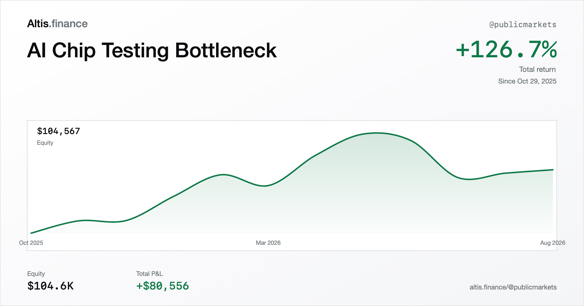
I started documenting the opportunity on October 29, 2025, through a portfolio covering seven companies across the testing process. Today, it is up 126.7%.
The portfolio has generated $80,556 in total profit on approximately $63,566 of original capital deployed. Around $25,577 has already been realized through partial sales, while $54,979 remains open.
The recent results support the original thesis, but the share prices now reflect far more optimism than they did last October. Several positions have doubled or tripled, which means the question is no longer whether AI is creating more demand for semiconductor testing. It is whether the remaining growth is enough to justify what investors are now paying for it.
Semiconductor testing is not one product or one market. The portfolio owns companies operating at five different points in the process.
Advantest and Teradyne manufacture the main testing platforms. These systems apply electrical signals to a chip, measure how it responds and determine whether it functions within the required specifications.
Their opportunity grows with both production volumes and complexity. More demanding chips require support for additional pins, higher data rates, greater parallelism and more complicated test programs.
The testing machine needs a physical interface to connect with the dies on a wafer. FormFactor and Technoprobe manufacture the customized probe cards that make those connections through microscopic contact points.
A modern probe card can contain more than 100,000 contacts, carry more than 1,000 amps and operate across extreme temperatures—all within an extraordinarily small physical space. As chip architectures change, manufacturers frequently need new, customized probe cards.
That close relationship with each new chip design gives this part of the portfolio a recurring element: a new architecture often requires a new interface rather than continued use of the old one.
During final testing, chips need to be moved into position, connected, heated or cooled, inspected and sorted without interrupting production. Cohu supplies much of this equipment. Its current systems can actively manage the heat generated by high-power AI processors, with a roadmap extending from 3 kilowatts toward 10 kilowatts of power dissipation. The company also provides HBM inspection equipment and software used to improve manufacturing yield.
Chroma ATE covers a broader part of the process, including semiconductor testing, power systems and system-level validation. This gives the portfolio exposure to faults that become visible only when the finished device is operated under conditions closer to those inside an AI server.
Amkor provides advanced packaging and outsourced semiconductor assembly and testing. Unlike the equipment companies, it is paid more directly on the volume of chips moving through production. Its margins are lower, but it offers exposure to the point where the different components become a finished device.
Owning all five layers was deliberate. I did not want the portfolio to depend on one company winning tester market share or one type of AI chip reaching production. I wanted exposure to the broader increase in testing complexity, wherever it appeared in the manufacturing process.
When I opened the first positions in October 2025, testing remained one of the less appreciated parts of the AI supply chain.
That is no longer true.
Several positions have doubled or tripled. The strongest companies now trade at valuations that assume AI testing demand remains exceptional for several years. Operational results are still improving, but entry prices have moved much faster than the original thesis.
I therefore started taking profits.
I sold roughly one-third of the FormFactor and Amkor positions in April, followed by partial sales of Teradyne, Cohu and Technoprobe at the end of June. These transactions realized approximately $25,577 while preserving exposure to every layer of the original thesis.
That distinction matters.
I have not exited because the testing bottleneck disappeared. The latest results suggest the opposite: it is becoming more visible.
I reduced because a correct thesis can become a poor new investment when the price starts assuming that nothing will go wrong.
Below the paywall, I will show:
all seven positions behind the +126.7% return;
the original entry price and position size for every holding;
every partial sale and the profit already realized;
which parts of the testing stack produced the strongest economics;
why I now prefer equipment and interfaces to outsourced assembly;
which companies still have the strongest operational momentum;
which positions have become the most vulnerable to a valuation reset;
and the exact signals I will use to add, reduce or exit as the thesis evolves.
Premium members will also be able to follow the portfolio on Altis Terminal, including its complete trade history, performance, future events and every new portfolio decision.
The newsletter explains why the bottleneck exists.
Terminal documents what happens after the thesis becomes obvious.
To access this portfolio — and all of our other live portfolios — subscribe to Public Markets Premium.
Altis Terminal will normally cost $499 per year as a standalone subscription. But full Terminal access is included with Public Markets Premium.
For $300 per year, you receive both:
every Public Markets Premium edition;
and complete access to Altis Terminal, where you can follow our portfolios, performance, trade histories, new positions and future updates in real time.
That means you receive the newsletter and Terminal together for $199 less than the future standalone price of Terminal alone.
Subscribe to Public Markets Premium for $300 per year and get Altis Terminal included.
Comments
Nothing yet. Say the first thing.
Sign in to join the conversation.