
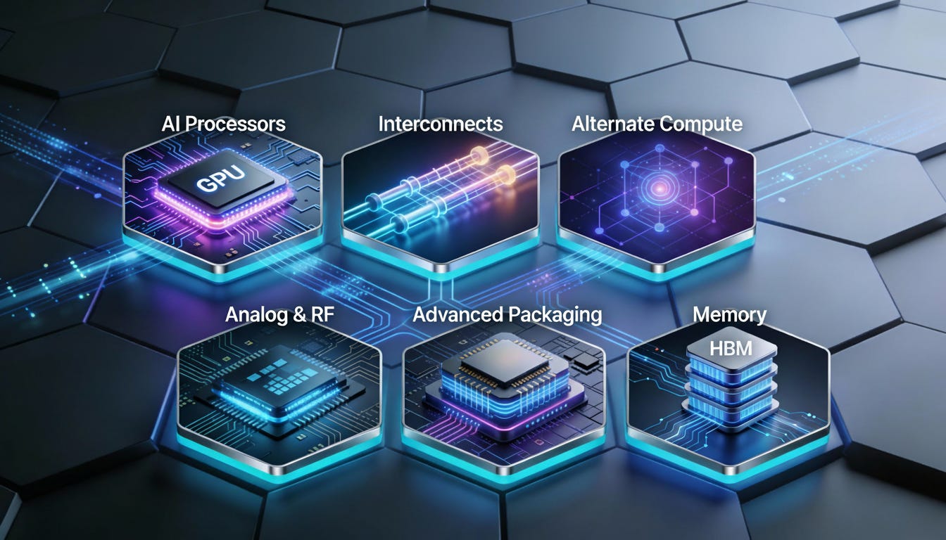
The semiconductor & compute industry is about to experience its biggest leap in a decade—and 2026 is when it all converges. While the world debates AI’s future, chipmakers are quietly engineering the hardware revolution that will define the next era of computing, including alternate computing like Quantum. From the first wave of 2nm processors hitting production lines to breakthrough memory technologies promising 600+ GB on a single stack, the silicon roadmap for 2026 reads like science fiction becoming reality.
What is interesting is not just the usual suspects like Apple and NVIDIA pushing boundaries—we’re seeing quantum processors approaching 1,000 logical qubits, optical interconnects delivering 114+ Tbps, and analog innovations that could slash power consumption by 100x for edge AI.
Here’s what’s actually shipping in 2026 across six pillars of Semiconductor industry, with a special segment for 2nm products, to showcase why the convergence of 2nm process nodes, HBM4 memory, and next-gen packaging might matter more than any single AI model launch this year.
Several companies are lining up first‑wave 2nm products for 2026, mostly on TSMC N2 and Samsung 2nm GAA. Below are five key expectations:
AMD EPYC “Venice” (Zen 6, 2 nm CCDs)— EPYC "Venice" server CPUs will use TSMC N2 for core‑complex dies (CCDs), with IO die on a mature node, improving performance‑per‑watt and core density for cloud and AI servers. AMD's first 2nm data‑center CPU generation, expected around 2026 as N2 capacity ramps. BTW, Zen-7 is already in cards now.
Apple A20 (2 nm iPhone SoC) — Apple A20 on TSMC N2, expected for 2026 iPhones. First Apple mobile SoC on gate‑all‑around (GAA) transistors, delivering 10–15% higher performance or up to 30% lower power versus N3. Targets higher on‑device AI throughput and better battery life within smartphone thermal limits.
Apple (again…) M6 (2 nm Mac SoC family) — Apple M6 family (Mac and iPad) on TSMC N2, among first wave of 2nm customers. Higher CPU/GPU density and efficiency from N2 plus upgraded Neural Engine for local generative AI workloads, transforming AI experiences
Apple leverages its priority allocation at TSMC, securing over half of early N2 capacity in 2026.
MediaTek Dimensity 9600‑class 2 nm SoC—MediaTek flagship 2nm SoC (Dimensity 9600 series) on TSMC N2, mass production targeted for late 2026. Uses 1.2× density boost to enlarge GPU and AI engines while maintaining all‑big‑core CPU strategy. Targets AI‑rich premium phones, PCs, and possibly automotive/edge compute with higher AI compute per watt.
Samsung Exynos 2600 (2 nm GAA)—Samsung Exynos 2600 on Samsung's own 2nm GAA process, mass‑production planned for 2026. Among first commercial chips on Samsung 2nm for mobile, expanding later to HPC/automotive.
This product will get benefitted from Samsung’s 2 nm ramp (including its Taylor, Texas fab) and tight coupling with HBM4 base‑die production for AI‑adjacent workloads.
AMD Instinct MI400 Series (CDNA 5) — AMD's 2026 refresh using CDNA 5 on 3nm, featuring HBM4 integration, improved matrix engines for inference and training, and Infinity Fabric Gen 5 for multi-GPU scaling. Enhanced thermal design for dense data-center packaging and broad ROCm ecosystem leverage.
Google 7th-Gen TPU with HBM4 — Google's next‑generation TPU adopting HBM4, delivering higher bandwidth and capacity for multi‑replica training and large‑batch inference on Google Cloud. Direct HBM4 integration maximizes memory bandwidth per die.
Intel Gaudi 3 / Crescent Island (volume production) — Intel's inference-optimized accelerator for cost-per-inference leadership, with custom tensor arrays and integrated high-speed fabric for cluster communication. Targets hyperscalers seeking NVIDIA/AMD alternatives with lower TCO for large-batch inference.
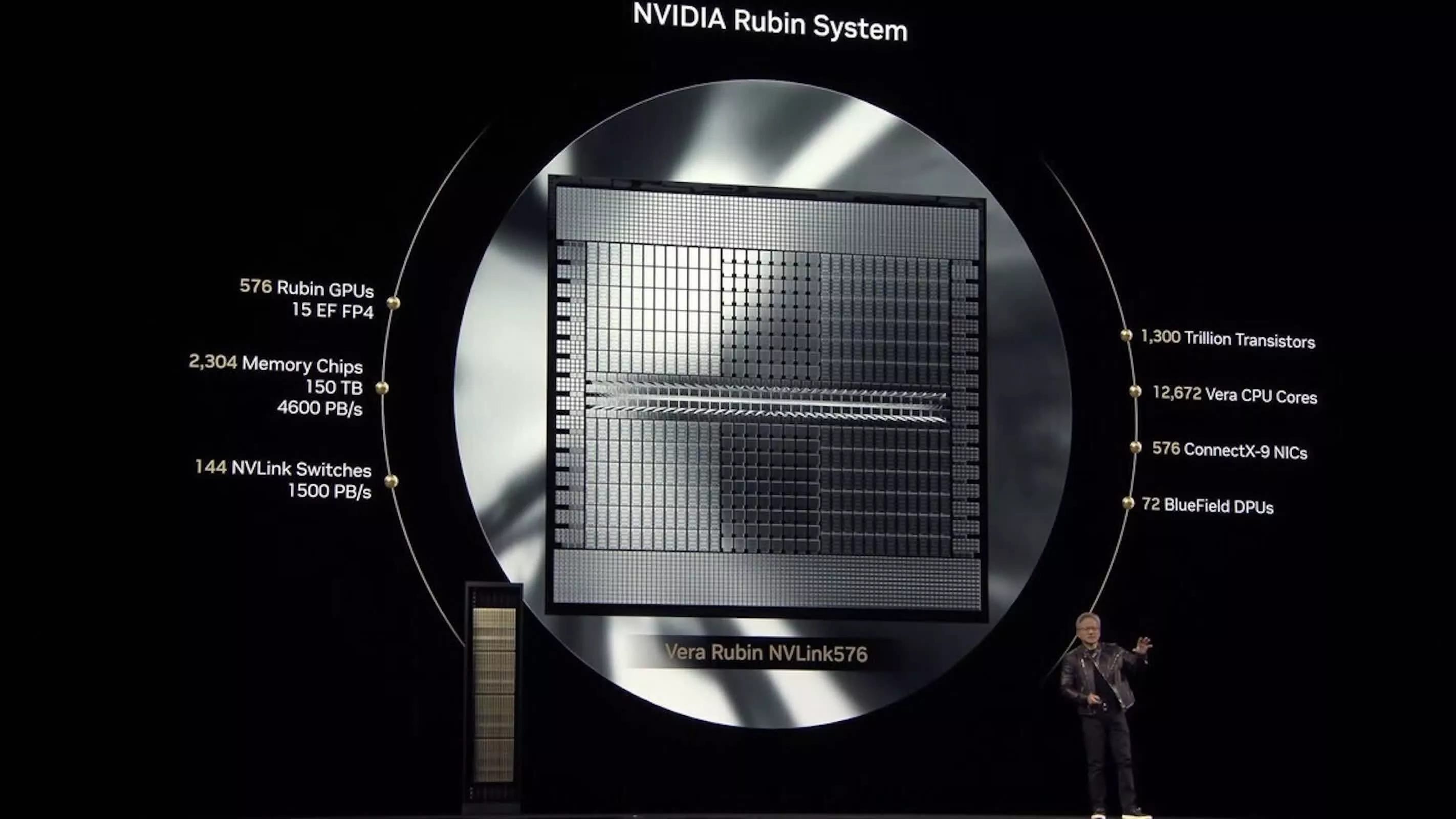
NVIDIA Rubin R100 GPU with HBM4 — Comprehensive overhaul of NVIDIA's compute infrastructure, spanning processors, networking, and interconnect technology. Designed on ~3nm, paired with HBM4 for increased on‑package capacity and bandwidth for multi‑trillion‑parameter models, including Grace‑Rubin superchips with higher‑bandwidth NVLink.
OpenAI Custom AI Processor (Broadcom-designed) — Bespoke accelerator built by Broadcom for OpenAI, optimized for OpenAI's proprietary training and inference algorithms. Innovation: vendor-agnostic custom silicon with potential architectural advantages over general-purpose GPUs
Broadcom’s involvement ncreases realization probability, but I will wait till the product comes, as there are lots of variables.
NVIDIA Quantum-X InfiniBand ASIC with Co-Packaged Optics (CPO) — InfiniBand switch ASIC with integrated silicon photonics, delivering 800 Gb/s per port with sub-microsecond latency, eliminating external optical pluggables. Monolithic optics-electronics integration reduces power consumption by ~10x versus discrete optics.
Broadcom Tomahawk 7 Ethernet Switch (12.8 Pbps) — Next-gen Ethernet ASIC with 512+ 400G/800G ports, sub-400ns latency, and cognitive routing optimized for AI cluster congestion control. Standards-based alternative to proprietary interconnects, addressing hyperscaler demand for open-source fabric options.
TSMC COUPE (Co-Packaged Optics) Platform — Though kind of packaging technique, this one enhances the interconnects we have today. TSMC’s advanced packaging platform integrating optical modules directly into foundry customer designs, enabling any chiplet vendor to add optical I/O via standardized design methodology. Democratizes optical interconnect access & reduces custom engineering costs.
Lightmatter Passage Optical Interconnect Chiplet (2026 ramp) — Silicon photonics chiplet delivering 114+ Tbps per module with nanosecond latency, enabling distributed memory architectures and connecting thousands of GPUs in single optical domain. Scales AI clusters without expensive long-reach fiber infrastructure.
Ayar Labs E-Series TeraPHY Optical I/O Chiplet (UCIe-compatible) — Standards-based (UCIe) optical chiplet offering 8+ Tbps bandwidth for chiplet-to-chiplet communication with sub-latency optical links. Reduces energy per data movement versus electrical and enables heterogeneous chiplet mixing.
Microsoft Azure Quantum Processor (topological qubits) — Next-gen topological quantum processor improving on Majorana architecture, targeting 1000+ logical qubits by mid-2027 with enhanced error correction. Topological qubits promise longer coherence times and natural error mitigation. I expect at least one release happening in 2026 to meet the ‘27 target.
IBM Quantum Kookaburra (multi-chip modular system) — Multi-chip quantum architecture supporting 1000+ logical qubits through distributed entanglement, improving scalability beyond single-chip constraints. Modular topology enables graceful scaling without physical die size limits.
Fujitsu Quantum Co-Processor (volume production ramp) — Commercial hybrid classical-quantum system with 256–500 superconducting qubits, cryogenic control electronics, and x86 CPU integration. Advantage: Japanese supply-chain sovereignty and tailored optimization/simulation workloads.
Neuromorphic Computing Platform (Intel Loihi 3 or successor) — Event-driven spiking neural network processor with 1000x lower power consumption versus traditional digital AI chips for specific inference tasks. Applications: edge AI, continuous sensor processing, autonomous robotics with extreme battery life.
Analog Inference Accelerator (specialized purpose) — Mixed-signal compute in analog domain (photonic neural networks, memristor arrays) for signal processing and sensor fusion with 10–100x power efficiency versus digital. Emerging category breaking from digital-only AI compute for edge and IoT.
ROHM 800 VDC DC-DC Controller and Gate Driver ICs — Integrated power-stage controllers and drivers for 12→48→800V isolated rail conversion in gigawatt-scale data centers, leveraging SiC/GaN MOSFETs. Reduces BOM complexity and improves thermal density for AI rack power architectures.
TI Multi-Phase Power Management ICs (AI Accelerator rails) — Integrated PMICs handling up to 6 voltage domains on single AI board, with integrated telemetry and sequencing, reducing external components and design cycle time. AI-specific power integration simplifies board design for 500+ W GPUs.
Infineon / ST SiC Gate‑Driver IC Families for EV & Renewable Inverters — Automotive‑qualified isolated gate drivers for SiC MOSFETs and IGBTs, with galvanic isolation, DESAT protection, high CMTI and fast propagation delays. Targets traction inverters, onboard chargers, and industrial/solar inverters.
RF Front-End Modules for 5G/mmWave (Sub-6 + FR2) — Integrated LNA, power amplifier, switch, and filter on single substrate with noise figure <1.5 dB and 50–100 dBm handling. Dense integration reduces parasitic coupling, shrinking form factor for IoT and mobile devices.
Automotive-Grade Battery Management ICs with integrated monitoring — Multi-cell monitors (up to 20 cells) with integrated coulomb counter, active cell balancing, and ISO 26262 L3 functional safety certification. Higher accuracy (±2% vs. ±10%) and integrated balancing simplify EV battery pack engineering.
SK hynix 2.5D HBM4 Turnkey Modules (2026 ramp) — Vertically integrated HBM4 stacks on silicon interposers with optional partner logic dies, thermally optimized for AI GPUs via Indiana manufacturing (2028 production ramp, 2026 early sampling). First turnkey HBM packaging outside TSMC CoWoS ecosystem, reducing customer integration risk and accelerating time-to-market.
TSMC CoWoS-X / CoWoS++ for HBM4 (high-density interposer) — Advanced CoWoS platform using hybrid bonding, denser routing, larger interposer dimensions (50+ mm sides), and 16-high HBM stack support. Hybrid bonding eliminates solder-bump microbumps, improving yield for large modules.
Micron HBM4 Packaging (Singapore & co‑located sites, 2026) — Micron ramping HBM4 volume production in 2026, building new HBM packaging facility in Singapore, with plans for Virginia co‑location. Strengthens vertical integration and offers alternative HBM4 supply alongside SK hynix and Samsung, improving AI memory supply chain resilience.
Fan‑Out Panel‑Level Packaging (FO‑PLP) for chiplets (2026 expansion) — FO‑PLP scales fan‑out wafer‑level packaging to large rectangular panels, improving area utilization and lowering cost per package for high‑volume AI and consumer devices. Panel‑scale and glass‑substrate adoption reduces dependence on silicon interposers.
Advanced Liquid Cooling and TIMs for 3D Packages — 2026 thermal roadmaps emphasize direct‑to‑chip and embedded liquid cooling, along with improved thermal interface materials, to manage rapidly rising heat flux in AI and 3D‑stacked devices.
TSMC and cooling vendors demonstrate direct‑to‑silicon and microchannel solutions handling hundreds of W/cm² – and in “some lab cases” approaching 1000 W/cm² – enabling higher‑power AI processors without throttling.
However, these may take till 2027 to get fully realized.
Samsung HBM4 Mass Production (6.4 GT/s, Feb 2026) — Third-generation high-bandwidth memory with 24–32 Gb dies, 16-high stack support (600+ GB per stack), 6.4 GT/s per pin (~1.2 TB/s bandwidth per stack), mass production starting February 2026. Breakthrough density and speed enable 800+ GB GPU modules for extreme-scale inference.
SK hynix HBM4 with Custom Base Die (2026) — HBM4 stacks with optional embedded logic on base die (cache, controller, protocol handler) using TSMC N5. Vendor-specific custom base dies reduce data movement and enable architectural optimizations for specific accelerator partners.
Micron HBM4 (N5 base die variant, 2026) — HBM4 with TSMC N5 base die, supporting non-NVIDIA customers (AMD, Google, others) with configurable bus width and speed options. Broadens HBM ecosystem beyond Samsung/SK hynix duopoly, supporting supply-chain diversification.
16-High HBM4 Stacks (600+ GB per module, late 2026) — Advanced stacking using improved through-silicon-via (TSV) processing and thermal management, enabling 16-high density (vs. 12-high in early HBM4). Extreme capacity supports models larger than GPU die footprint and context windows exceeding 1 million tokens.
HBM4E Roadmap (early deployments ~2026–2027) — HBM4E maintains 2,048‑bit interface while increasing per‑pin data rates from 8 Gb/s to ~12 Gb/s, raising bandwidth toward ~3 TB/s per stack with improved power and area efficiency versus HBM3E. TSMC and GUC offer customizable logic‑node base dies (down to 3nm) and custom die‑to‑die interfaces, letting GPU/accelerator vendors integrate memory‑controller and cache logic into base die and attach more stacks per package.
Memory remains a hot topic, including as a critical factor in consumer electronics pricing (laptops, gaming devices).
The timing of the next tech revamp will be interesting to watch. HBM5 (beyond 2026) is in cards now. Research and vendor roadmaps place HBM5 after HBM4E, around 2029, with similar per‑pin speeds but higher I/O counts (e.g., ~4096‑bit) to reach roughly 4 TB/s per stack, plus additional 3D cache and logic integration.
Thats all for this time. . .
Thanks a lot for reading Innovation Snaps. Please comment, share & follow me, for more stories on Innovation & Deep Tech. Though tried my best to avoid mistakes, please remit for any typos/mistakes.
No posts
Comments
Nothing yet. Say the first thing.
Sign in to join the conversation.