
For decades, chip engineers chased one direction: smaller. Shrink the transistor, pack more onto the same flat surface, keep Moore’s Law alive. Then came the wall, quantum effects, heat, physics that won’t negotiate. This week, a team led by professor Qing Cao at the University of Illinois Urbana-Champaign published a paper in Nature showing they can now stack fully functional silicon transistors directly on top of one another, layer by layer, with near-perfect yields of 98–100%.
The trick is doing it at low temperatures, low enough that the circuits already on the wafer survive the process. That has been the stumbling block for years. Other research groups have managed vertical integration with exotic materials or at temperatures that destroy previous layers. The Illinois team used standard single-crystalline silicon and kept the thermal budget tight enough to make the approach industrially viable.
The implications go well beyond doubling density. Vertical stacking shortens the wires between different parts of a chip, which cuts the parasitic capacitance that slows down signal travel and wastes energy. For AI accelerators, which need to shuffle enormous amounts of data between logic and memory, that kind of bandwidth improvement matters as much as raw compute.
This is what post-silicon computing actually looks like, not a new material, but a new geometry, built from the same silicon we already know how to make.
IBM, Intel, and TSMC are already listed as industry partners on the project. The researchers are now preparing to transfer the process to an industrial foundry. Three companies that together represent the majority of the world’s advanced chip manufacturing are invested in making this work. That is not preliminary research. That is a roadmap.
WHY IT MATTERS
Stacking silicon transistors vertically, not with exotic materials, but with standard silicon at manufacturable temperatures, breaks the ceiling that has slowed the chip industry for a decade and could multiply the performance of every AI accelerator built in the next five years. It also will greatly amplify the logic folding approach put forward by Huwaei to match the lower nm node process which they don’t have access.
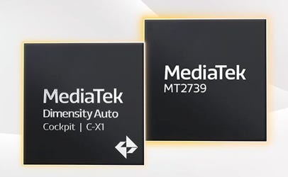
Mediatek’s Automotive AI Cockpit Platform - Dimensity AX C-X1 : 80 TOPS edge AI compute, 12-core CPU, 10.2 TFLOP GPU on a 3nm process. First car chip with NVIDIA GPU integration for AAA gaming and advanced driver HMI. Alongside it, the Dimensity AX MT2739, the world’s first automotive chip supporting 3GPP R18 5G satellite video calls. The car dashboard is becoming an AI workstation.
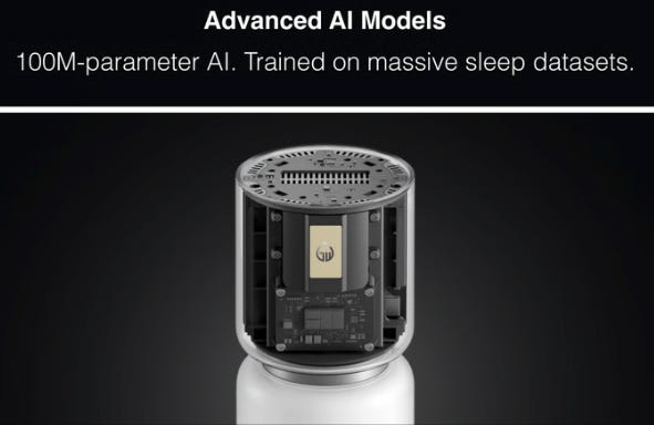
Sleepal AI Lamp, Contactless Sleep Tracker and Regulator : Sits on a bedside table, uses radar-based sensing with no wearable required, tracks sleep stages all night, and adjusts light spectrum and intensity to guide the body toward better sleep architecture. No subscription. All data stored locally. Sleep science without anything on your body or in your cloud account.
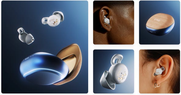
SOND Dreambuds, 12-Signal AI Sleep Earbuds : Monitors 12 physiological signals during sleep, including EEG-adjacent brainwave proxies, heart rate, SpO2, and movement. It then adapts audio environments in real time to deepen sleep stages. In-ear form factor, medical-grade sensing. Earbuds that learn how you sleep in order to change how you sleep.
NVIDIA RTX Spark Superchip : Announced at Computex 2026. Blackwell RTX GPU with 6,144 CUDA cores delivering 1 petaflop of AI performance, paired with a custom 20-core Grace CPU built with MediaTek and connected via NVLink. Targets slim Windows laptops and compact desktops for personal AI agents. NVIDIA’s first PC processor, 33 years after founding, that seems to be having a better prospect.
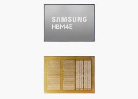
Samsung ships first samples of HBM4E 12-Layer Memory : World’s first 12-layer HBM4E samples shipped to Nvidia, AMD, and Google. 3.6 TB/s bandwidth per stack, over 20% faster than HBM4. Stable 14 Gbps pin speed with headroom to 16 Gbps. The memory chip that next-generation AI accelerators will depend on.
Intel’s Panther Lake Handheld Chip - Arc G3 & Arc G3 Extreme : Intel’s first chips designed specifically for gaming handhelds, built on 18A process with Panther Lake architecture. 25W base TDP, up to 80W max turbo. First Intel 18A products outside laptops; signals the US-made 1.8nm node moving into new markets. Intel 18A leaves the laptop and enters the gaming handheld.
3D Packaged AI Chips gets 4× efficient thermal solution. Engineered gold metamaterials enable near-field radiative heat transfer across nanoscale gaps at four times conventional rates by exploiting geometry-driven quantum effects. This bypasses thermal limits in advanced packaging. Improved nanoscale heat dissipation allows denser AI accelerators and 3D-stacked chips, increasing performance before thermal throttling constrains next-generation semiconductor systems.
A chip that processes light, steers it, and reads it back, all in one device : Scientists at Monash University built the first nanoscale circuit to generate, direct, and detect light-based information on a single chip, using a field of research called valleytronics. Previous work could do one or two of those things, never all three on one platform. The new device stacks atomically thin materials on engineered nanostructures, running at room temperature without the cryogenic cooling most quantum technologies require.
A Terahertz Detector from common semiconductor line : A quantum metasurface detector has closed the long-standing terahertz sensing gap by achieving high responsivity (2.7 amperes per watt at 1.9 THz) at room-useful conditions without bulky optics. Built using standard semiconductor processes, it enables compact, scalable terahertz imaging chips, unlocking affordable applications in security screening, medical diagnostics, and semiconductor defect inspection across industries worldwide today globally.
After 20 years, a laser that once filled a room fits inside a coin sized chip. EPFL researchers integrated a femtosecond Mamyshev oscillator laser onto a chip, delivering 1.05 nanojoules per 147 femtosecond pulse, matching tabletop systems. Using nonlinear waveguides and offset filters, it eliminates complex alignment. This coin-sized, manufacturable device enables chip-scale optical clocks, precision surgery, and embedded ultrafast sensing in autonomous and industrial systems.
A brain-inspired chip that fires like a neuron near absolute zero. A programmable neuromorphic chip using silicon carbide MOSFETs operates at 10 millikelvin, mimicking neuron-like spiking via negative differential resistance. Designed for quantum environments, it functions where conventional electronics fail. This enables integrated control within quantum systems, potentially replacing complex room-temperature hardware and advancing scalable quantum computing and deep-space electronics
Apple’s first approved AI Agent : has approved Poke as the first third-party AI agent on its Messages for Business platform. The text-based agent supports tasks like scheduling, smart-home control, and photo editing, and has processed over 100 million messages. Backed by $25M funding, valued at $300M, Poke pays Apple per-user, signaling a new monetization model for AI distribution and faces approval timelines of months.

AI-designed universal coronavirus vaccine passes first human trial. The vaccine targeting conserved features across the Sarbecovirus family showed safety and broad immune responses in Phase 1 trials. Developed by Scientists at the University of Cambridge and spin-out DIOSynVax, it is delivered needle-free, it avoids strain-specific design. This approach could provide preemptive protection against future coronaviruses, reducing reliance on variant-matched vaccines and improving pandemic preparedness globally.
Humanoid robots enter scaled deployment, as Figure 03 reaches one unit per hour production with over 500 shipped, while Boston Dynamics’ Atlas begins deliveries. High manufacturing yields and growing fleets accelerate AI learning via real-world data. This feedback loop drives rapid capability gains, pushing humanoids toward industrial-scale adoption and transforming physical AI economics.
Stanford trains humanoid robots using human motion data. Stanford researchers train vision-language-action models on real human demonstrations rather than simulation, learning directly from observed motion and visual context. This improves performance in manipulation tasks where synthetic data falls short. The approach reduces the reality gap, enabling more reliable deployment of humanoid robots in real-world environments.
NASA’s X-59 achieves first “quiet” supersonic flight. The X-59 reached Mach 1.077 at 43,000 feet, demonstrating low-boom “quiet thump” technology designed to replace disruptive sonic booms. Built to inform regulation, upcoming community overflights will gather noise-response data. The programme could enable lifting the US ban on overland supersonic travel, unlocking commercial high-speed aviation markets.

NASA demonstrates roaming between satellite networks in orbit. NASA’s PExT mission enabled spacecraft to switch between multiple relay networks using Ka-band links, including TDRS, Viasat, and SES. This dynamic connectivity improves data transmission efficiency and reduces blackout periods. The capability supports data-intensive lunar and deep-space missions, enabling more reliable, flexible communications across heterogeneous space networks.
Artemis III crew is named for pre-landing mission. NASA selected Randy Bresnik, Luca Parmitano, Frank Rubio, and Andre Douglas for Artemis III, a 2027 mission focused on orbital rendezvous and docking with commercial lunar landers. This pre-landing validation is critical for Artemis IV’s 2028 Moon landing, making crew readiness and system integration central to programme success.
JWST reveals distinct dawn and dusk atmospheres on exoplanet. Using JWST, researchers observed different atmospheric conditions on the morning and evening sides of WASP-121b, detecting key molecules and temperature asymmetry driven by extreme winds. This first confirmation of predicted terminator differences validates atmospheric models and improves our ability to interpret exoplanet climates and potential habitability.
Battery Free Artificial Photosynthesis system : Researchers developed a system that eliminates batteries using a self-regulating electrolyzer that adjusts resistance with sunlight intensity, stabilizing fuel production. It converts CO₂ and water into formic acid, a storable liquid fuel. This low-complexity design reduces cost and maintenance, enabling practical deployment in off-grid and resource-constrained environments.
Food-waste-derived beads capture CO₂ from air efficiently. ETH Zurich researchers created biodegradable beads from dairy and tofu waste proteins that capture CO₂ using potassium hydroxide. The system achieves 2.20 mmol per gram and regenerates at room temperature without energy-intensive heating. This low-cost, circular approach enables distributed carbon capture at agricultural and food-processing sites.
Solar desalination system produces water and recovers lithium. Researchers developed a solar desalination system using superwicking black metal surfaces to generate drinking water while recovering solid salts, including lithium. By eliminating liquid brine waste, it combines water purification with resource extraction, offering a scalable solution for water scarcity and critical battery material supply challenges.
Thanks a lot for reading Innovation Snaps.
Please share your comments & this newsletter if you enjoyed it. Though tried my best to avoid mistakes, please remit for any typos/mistakes.
No posts
Comments
Nothing yet. Say the first thing.
Sign in to join the conversation.